LSTTL input logic compatible
VIL(max) = 0.8 V, VIH(min) = 2 V
CMOS input logic compatible
II ≤ 1 µA at VOL, VOH
Buffered inputs
4.5 V to 5.5 V operation
Wide operating temperature range:
-55°C to +125°C
Supports fanout
Full PDF Text Transcription for CD74HCT20 (Reference)
Note: Below is a high-fidelity text extraction (approx. 800 characters) for
CD74HCT20. For precise diagrams, and layout, please refer to the original PDF.
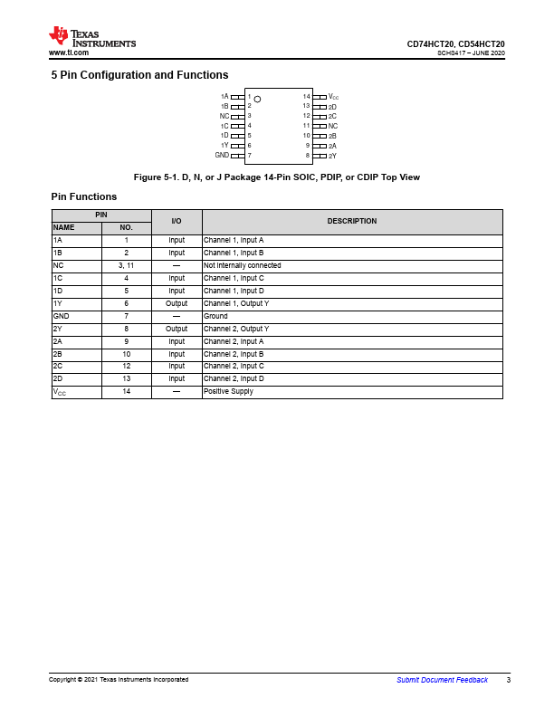
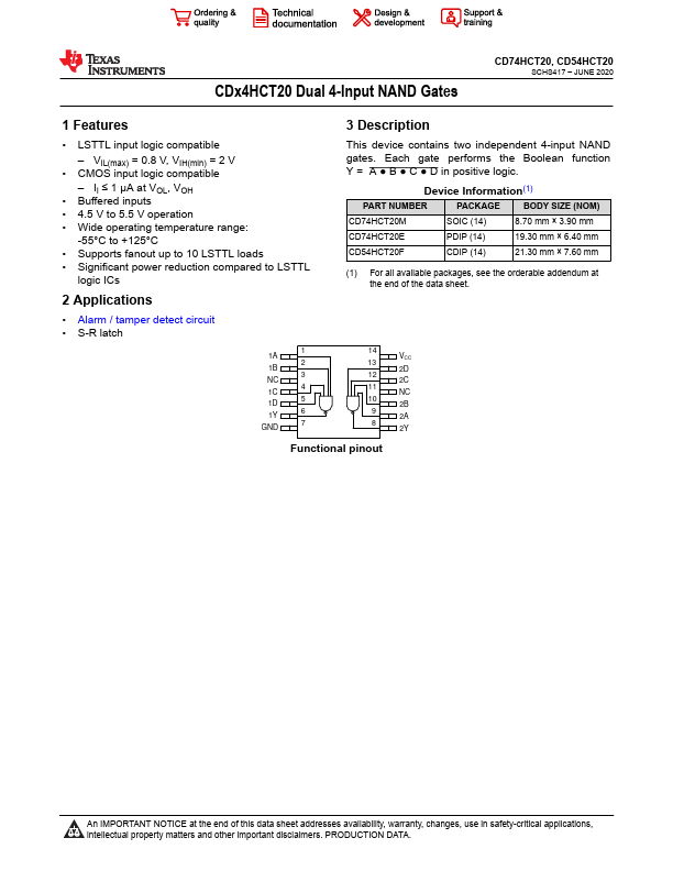
• LSTTL input logic compatible – VIL(max) = 0.8 V, VIH(min) = 2 V • CMOS input logic compatible – II ≤ 1 µA at VOL, VOH • Buffered inputs • 4.5 V to 5.5 V operation • Wide operating temperature range: -55°C to +125°C • Supports fanout up to 10 LSTTL loads • Significant power reduction compared to LSTTL logic ICs 2 Applications This device contains two independent 4-input NAND gates. Each gate performs the Boolean function Y = A ● B ● C ● D in positive logic. Device Information(1) PART NUMBER PACKAGE BODY SIZE (NOM) CD74HCT20M SOIC (14) 8.70 mm × 3.90 mm CD74HCT20E PDIP (14) 19.30 mm × 6.40 mm CD54HCT20F CDIP (14) 21.30 mm
 CD74HCT20 Datasheet