Datasheet4U Logo Datasheet4U.com

74SSTUB32864A - 25-Bit Configurable Registered Buffer

Description

This 25-bit 1:1 or 14-bit 1:2 configurable registered buffer is designed for 1.7-V to 1.9-V VCC operation.

In the 1:1 pinout configuration, only one device per DIMM is required to drive nine SDRAM loads.

In the 1:2 pinout configuration, two devices per DIMM are required to drive 18 SDRAM loads.

Features

  • Member of the Texas Instruments Widebus+™ Family.
  • Pinout Optimizes DDR2 DIMM PCB Layout.
  • Configurable as 25-Bit 1:1 or 14-Bit 1:2 Registered Buffer.
  • Chip-Select Inputs Gate the Data Outputs from Changing State and Minimizes System Power Consumption.
  • Output Edge-Control Circuitry Minimizes Switching Noise in an Unterminated Line.
  • Supports SSTL_18 Data Inputs.
  • Differential Clock (CLK and CLK) Inputs.
  • Supports LVCMOS Switchin.

📥 Download Datasheet

Full PDF Text Transcription

Click to expand full text
74SSTUB32864A www.ti.com 25-BIT CONFIGURABLE REGISTERED BUFFER SCAS838 – OCTOBER 2006 FEATURES • Member of the Texas Instruments Widebus+™ Family 
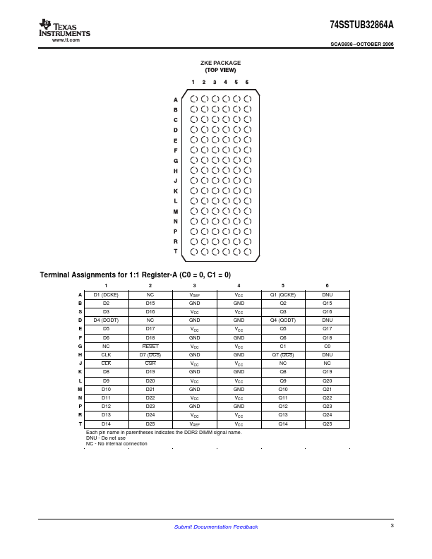
• Pinout Optimizes DDR2 DIMM PCB Layout • Configurable as 25-Bit 1:1 or 14-Bit 1:2 Registered Buffer • Chip-Select Inputs Gate the Data Outputs from Changing State and Minimizes System Power Consumption • Output Edge-Control Circuitry Minimizes Switching Noise in an Unterminated Line • Supports SSTL_18 Data Inputs • Differential Clock (CLK and CLK) Inputs • Supports LVCMOS Switching Levels on the Control and RESET Inputs • RESET Input Disables Differential Input Receivers, Resets All Registers, and Forces All Outputs Low DESCRIPTION This 25-bit 1:1 or 14-bit 1:2 configurable registered buffer is designed for 1.7-V to 1.9-V VCC operation.
Published: |