Click to expand full text
• Independent Registers and Enables for A
and B Buses
• Multiplexed Real-Time and Stored Data • Inverting Data Paths • Flow-Through Architecture Optimizes PCB
Layout
• Center-Pin VCC and GND Configurations
Minimize High-Speed Switching Noise
• EPIC (Enhanced-Performance Implanted
CMOS) 1-µm Process
• 500-mA Typical Latch-Up Immunity at
125°C
• Package Options Include Plastic
Small-Outline Packages and Standard Plastic 300-mil DIPs
description
74AC11651 OCTAL BUS TRANSCEIVER AND REGISTER
WITH 3ĆSTATE OUTPUTS
SCAS135 − MARCH 1990 − REVISED APRIL 1993
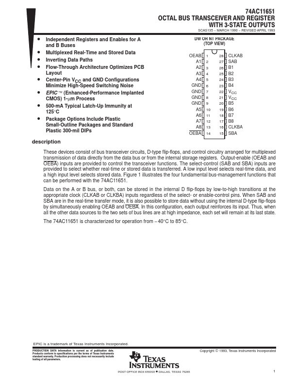
DW OR NT PACKAGE (TOP VIEW)
OEAB A1 A2 A3 A4
GND GND GND GND
A5 A6 A7 A8 OEBA
1 2 3 4 5 6 7 8 9 10 11 12 13 14
28 CLKAB 27 SAB 26 B1 25 B2 24 B3 23 B4 22 VCC 21 VCC 20 B5 19 B6 18 B7 17 B8 16 CLKBA 15 SBA
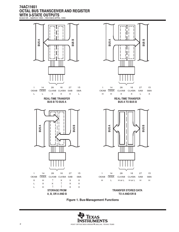
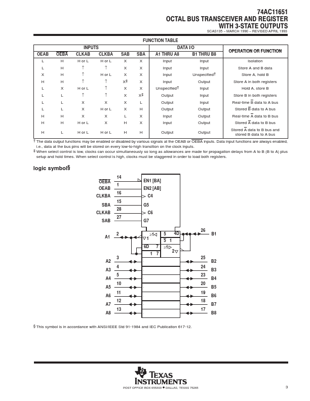
These devices consist of bus tran
 74AC11651 Datasheet