Click to expand full text
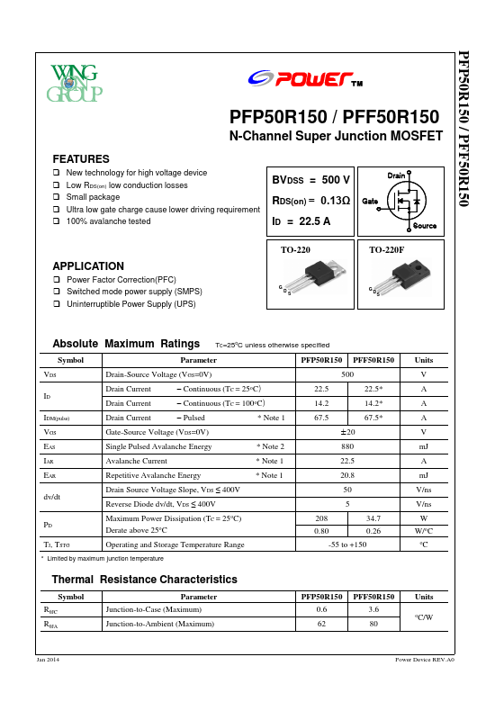
PFP50R150 / PFF50R150
PFP50R150 / PFF50R150
N-Channel Super Junction MOSFET
FEATURES
New technology for high voltage device Low RDS(on) low conduction losses Small package Ultra low gate charge cause lower driving requirement 100% avalanche tested
BVDSS = 500 V RDS(on) = 0.13Ω ID = 22.5 A
Drain
Gate
●
◀▲
● ●
Source
APPLICATION
Power Factor Correction(PFC) Switched mode power supply (SMPS) Uninterruptible Power Supply (UPS)
TO-220
G DS
TO-220F
G DS
Absolute Maximum Ratings TC=25oC unless otherwise specified
Symbol
Parameter
PFP50R150 PFF50R150
VDS
ID
IDM(pulse) VGS
Drain-Source Voltage (VGS=0V)
Drain Current
– Continuous (TC = 25oC)
Drain Current
– Continuous (TC = 100oC)
Drain Current
– Pulsed
* Note 1
Gate-Source Voltage (VDS=0V)
500 22.5 22.
 PFF50R150 Datasheet