Si4824DY
FEATURES
D High-Efficiency D PWM Optimized D 100% Rg Tested
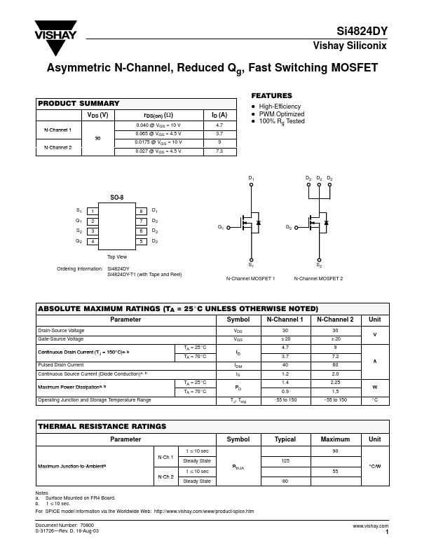
S1 1 G1 2 S2 3 G2 4
SO-8
8 D1 7 D2 6 D2 5 D2
Top View
Ordering Information: Si4824DY Si4824DY-T1 (with Tape and Reel)
D1
D2 D2 D2
G1
G2
S1 N-Channel MOSFET 1
S2 N-Channel MOSFET 2
ABSOLUTE MAXIMUM RATINGS (TA = 25_C UNLESS OTHERWISE NOTED)
Parameter
Symbol
N-Channel 1 N-Channel 2
Drain-Source Voltage Gate-Source Voltage
Continuous Drain Current (TJ = 150_C)a, b Pulsed Drain Current Continuous Source Current (Diode Conduction)a, b
Maximum Power Dissipationa, b Operating Junction and Storage Temperature Range
TA = 25_C TA = 70_C
TA = 25_C TA = 70_C
VDS VGS
ID IDM IS
PD TJ, Tstg
30 "20 4.7 3.7 40 1.2 1.4 0.9
- 55 to 150
30 "20
9 7.2 60 2.0 2.25 1.5
- 55 to 150
Unit
W _C
THERMAL RESISTANCE RATINGS
Parameter
Symbol
Maximum Junction-to-Ambienta
N-Ch 1 N-Ch 2 t v10 sec Steady State t v10 sec Steady State
Rth...