Click to expand full text
VBL2606
www.VBsemi.com
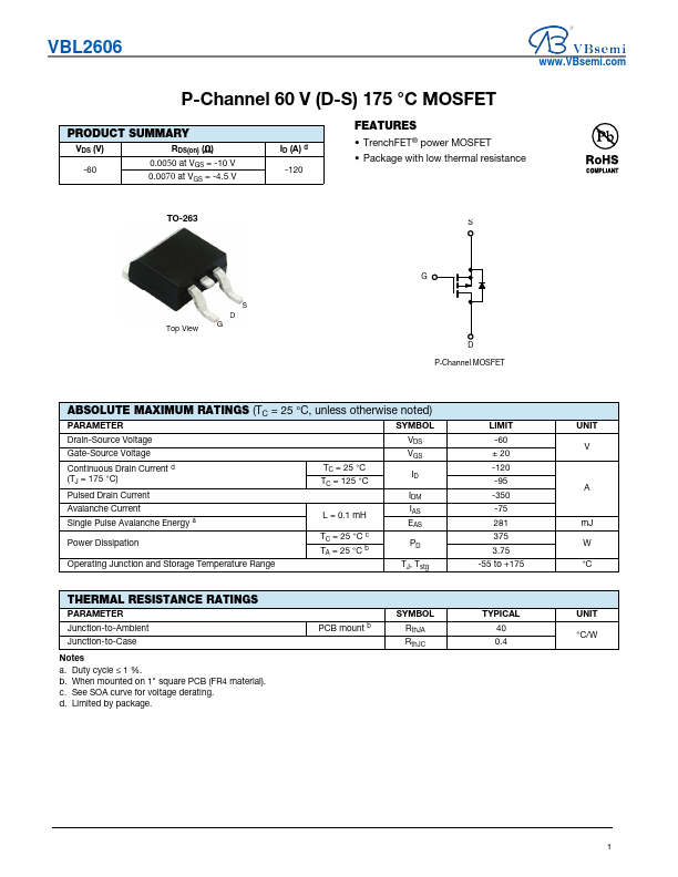
P-Channel 60 V (D-S) 175 °C MOSFET
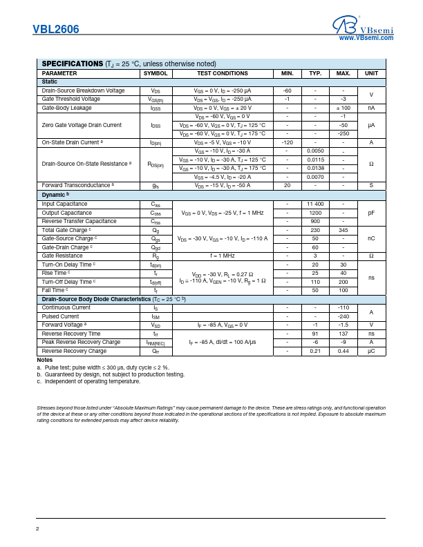
PRODUCT SUMMARY
VDS (V)
RDS(on) (Ω)
-60
0.0050 at VGS = -10 V
0.0070 at VGS = -4.5 V
ID (A) d -120
FEATURES • TrenchFET® power MOSFET • Package with low thermal resistance
TO-263
S
Top View
S D G
G
D P-Channel MOSFET
ABSOLUTE MAXIMUM RATINGS (TC = 25 °C, unless otherwise noted)
PARAMETER
SYMBOL
Drain-Source Voltage
VDS
Gate-Source Voltage
VGS
Continuous Drain Current d (TJ = 175 °C)
TC = 25 °C TC = 125 °C
ID
Pulsed Drain Current
IDM
Avalanche Current Single Pulse Avalanche Energy a
Power Dissipation
L = 0.1 mH
IAS
EAS
TC = 25 °C c TA = 25 °C b
PD
Operating Junction and Storage Temperature Range
TJ, Tstg
THERMAL RESISTANCE RATINGS
PARAMETER Junction-to-Ambient Junction-to-Case
Notes a.
 VBL2606 Datasheet