Click to expand full text
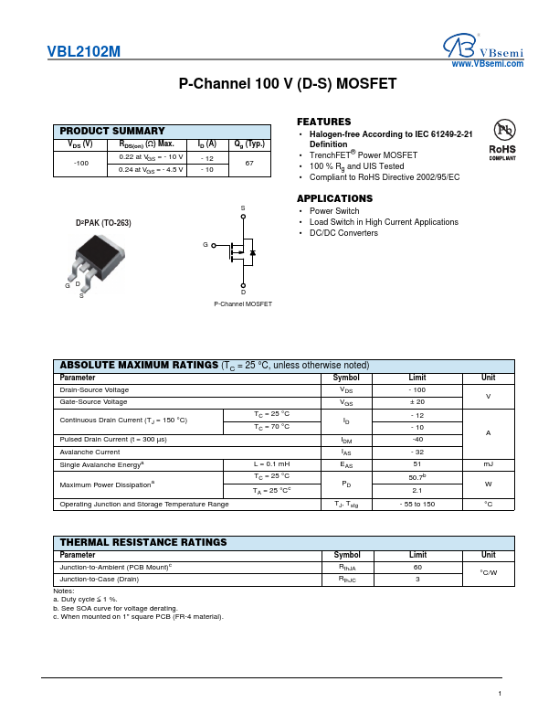
VBL2102M
P-Channel 100 V (D-S) MOSFET
www.VBsemi.com
PRODUCT SUMMARY
VDS (V)
RDS(on) () Max.
-100
0.22 at VGS = - 10 V 0.24 at VGS = - 4.5 V
ID (A) - 12 - 10
Qg (Typ.) 67
D2PAK (TO-263)
S G
FEATURES • Halogen-free According to IEC 61249-2-21
Definition • TrenchFET® Power MOSFET • 100 % Rg and UIS Tested • Compliant to RoHS Directive 2002/95/EC
APPLICATIONS • Power Switch • Load Switch in High Current Applications • DC/DC Converters
GD S
D P-Channel MOSFET
ABSOLUTE MAXIMUM RATINGS (TC = 25 °C, unless otherwise noted)
Parameter
Symbol
Drain-Source Voltage
VDS
Gate-Source Voltage
VGS
Continuous Drain Current (TJ = 150 °C)
TC = 25 °C TC = 70 °C
ID
Pulsed Drain Current (t = 300 µs)
IDM
Avalanche Current
IAS
Single Avalanche Energya
L = 0.
 VBL2102M Datasheet