Click to expand full text
VBBD4290
Dual P-Channel 20 V (D-S) MOSFET
www.VBsemi.com
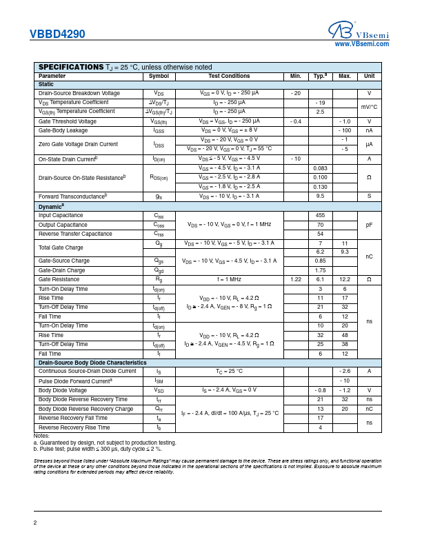
PRODUCT SUMMARY
VDS (V)
RDS(on) (Ω)
0.083 at VGS = - 4.5 V
- 20
0.100 at VGS = - 2.5 V
0.130 at VGS = - 1.8 V
DFN 3x2
ID (A)a - 4g - 4g - 3.8
Qg (Typ.) 6.2 nC
1
S1
D1 D1
G1 S2
D2
G2
D2
FEATURES
• Halogen-free According to IEC 61249-2-21 Definition
• TrenchFET® Power MOSFETs
• 100 % Rg Tested • Compliant to RoHS Directive 2002/95/EC
APPLICATIONS • Load Switch for Portable Devices • Battery Switch
S1
S2
G1
G2
Bottom View
D1 P-Channel MOSFET
D2 P-Channel MOSFET
ABSOLUTE MAXIMUM RATINGS TA = 25 °C, unless otherwise noted
Parameter
Symbol
Limit
Unit
Drain-Source Voltage Gate-Source Voltage
VDS
- 20
VGS
±8
V
TC = 25 °C
- 4g
Continuous Drain Current (TJ = 150 °C)
TC = 70 °C TA = 25 °C
ID
- 3.
 VBBD4290 Datasheet