J603
FEATURES
- Halogen-free According to IEC 61249-2-21
Definition
- Trench Power MOSFET
- 100 % Rg and UIS Tested
- pliant to Ro HS Directive 2002/95/EC
APPLICATIONS
- Power Switch
- Load Switch in High Current Applications
- DC/DC Converters
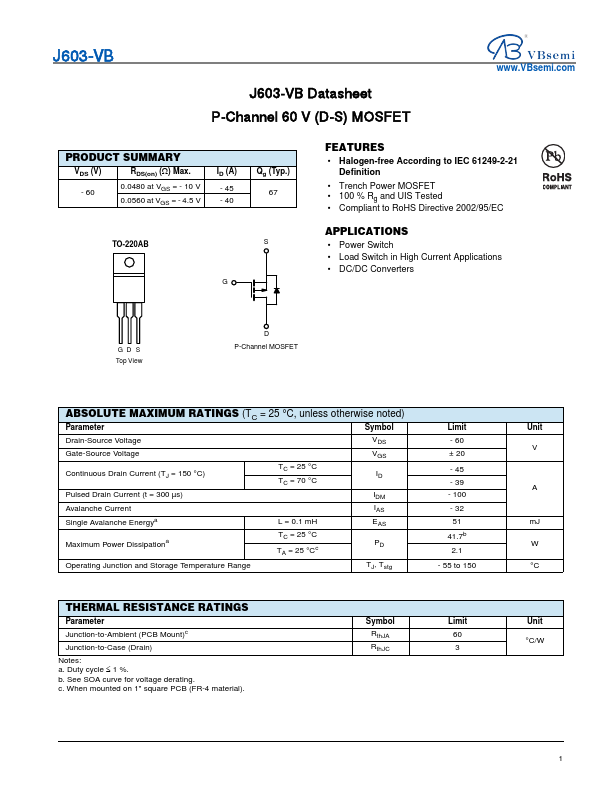
GD S Top View
D P-Channel MOSFET
ABSOLUTE MAXIMUM RATINGS (TC = 25 °C, unless otherwise noted)
Parameter
Symbol
Drain-Source Voltage
Gate-Source Voltage
Continuous Drain Current (TJ = 150 °C)
TC = 25 °C TC = 70 °C
Pulsed Drain Current (t = 300 µs)
Avalanche Current
Single Avalanche Energya
L = 0.1 m H
Maximum Power Dissipationa
TC = 25 °C
TA = 25 °Cc
Operating Junction and Storage Temperature Range
TJ, Tstg
Limit
- 60 ± 20
- 45
- 39
-...