Click to expand full text
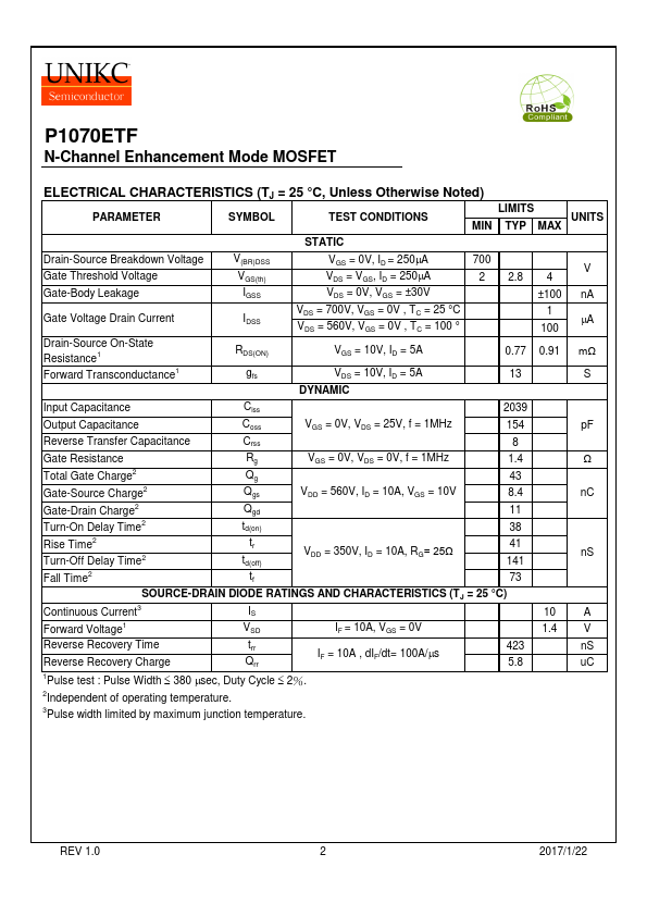
P1070ETF
N-Channel Enhancement Mode MOSFET
PRODUCT SUMMARY
V(BR)DSS
RDS(ON)
ID
700V
0.91mΩ @VGS = 10V
10A
TO-220F
100% UIS tested
ABSOLUTE MAXIMUM RATINGS (TA = 25 °C Unless Otherwise Noted)
PARAMETERS/TEST CONDITIONS
SYMBOL
LIMITS
Drain-Source Voltage
VDS
700
Gate-Source Voltage
VGS
±30
Continuous Drain Current2,4
Pulsed Drain Current1,2 Avalanche Current3 Avalanche Energy3
TC = 25 °C TC = 100 °C
ID
10 6
IDM
30
IAS
5
EAS
125
Power Dissipation
TC = 25 °C
PD
46
TC = 100 °C
18
Operating Junction & Storage Temperature Range
Tj, Tstg
-55 to 150
UNITS V
A
mJ W °C
THERMAL RESISTANCE RATINGS
THERMAL RESISTANCE
SYMBOL
Junction-to-Case
RqJC
Junction-to-Ambient
RqJA
1Pulse width limited by maximum junction temperature.
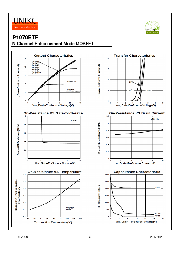
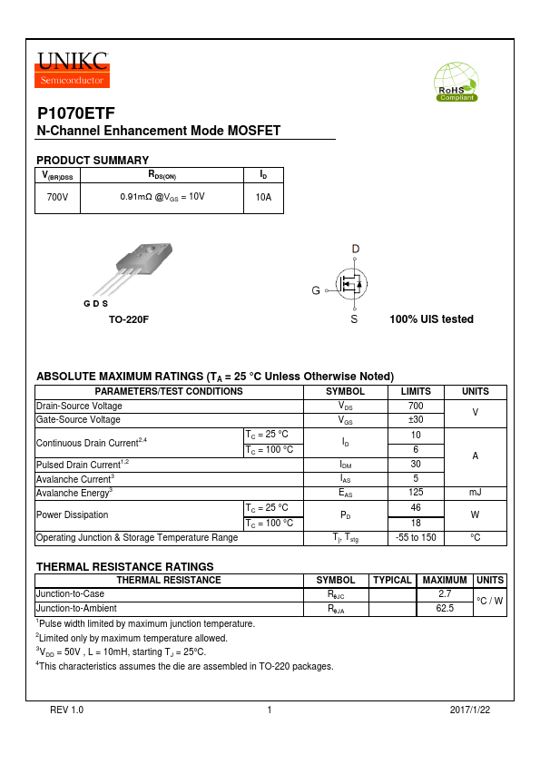
 P1070ETF Datasheet