AO3414A
Features
VDS (V) = 20V ID = 4.2A (VGS=4.5V) RDS(ON) 26m (VGS = 4.5V) RDS(ON) 36m (VGS = 2.5V) RDS(ON) 57m (VGS = 1.8V)
UMW AO3414A
N-Channel Enhancement MOSFET
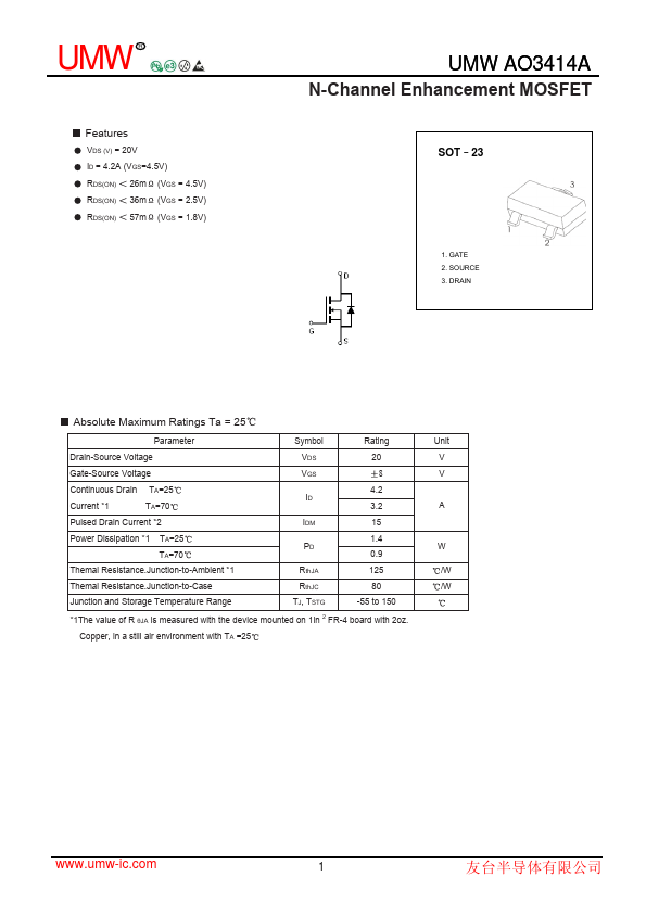
SOT- 23
1. GATE 2. SOURCE 3. DRAIN
Absolute Maximum Ratings Ta = 25
Parameter
Symbol
Rating
Drain-Source Voltage
Gate-Source Voltage
Continuous Drain TA=25
Current
- 1
TA=70
4.2 ID
Pulsed Drain Current
- 2
Power Dissipation
- 1 TA=25 TA=70
1.4 PD
Themal Resistance.Junction-to-Ambient
- 1
Rth JA
Themal Resistance.Junction-to-Case
Rth JC
Junction and Storage Temperature Range
TJ, TSTG
-55 to 150
- 1The value of R θJA is measured with the device mounted on 1in 2 FR-4 board with 2oz.
Copper, in a still air environment with TA =25
Unit V...