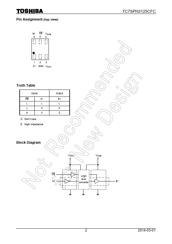
TC7SPN3125CFC TOSHIBA Digital Integrated Circuit Silicon Monolithic TC7SPN3125CFC Low Voltage/Low Power 1-Bit Dual Supply Bus Buffer The TC7SPN3125 is an advanced high-sp...
View more extracted text
wer 1-Bit Dual Supply Bus Buffer The TC7SPN3125 is an advanced high-speed CMOS 1-bit dual supply voltage interface bus buffer fabricated with silicon gate CMOS technology. It is also designed with over voltage tolerant inputs and outputs up to 3.6 V. Designed for use as an interface between a 1.2-V, 1.5-V, 1.8-V, or 2.5-V bus and a 1.8-V, 2.5-V or 3.3-V bus in mixed 1.2-V, 1.5-V, 1.8-V or 2.5-V/1.8-V, 2.5-V or 3.3-V supply systems. The A-input interfaces with the 1.2-V, 1.5-V, 1.8-V or 2.5-V bus, the B-output with the 1.8-V, 2.5-V, 3.3-V bus. The enable input ( OE ) can be used to disable the device so that the signal line
 TC7SPN3125CFC Datasheet