Full PDF Text Transcription for TC7SP57FU (Reference)
Note: Below is a high-fidelity text extraction (approx. 800 characters) for
TC7SP57FU. For precise diagrams, and layout, please refer to the original PDF.
TC7SP57,58FU TOSHIBA CMOS Digital Integrated Circuit Silicon Monolithic TC7SP57FU, TC7SP58FU Low Voltage Single Configurable Multiple Function Gate with 3.6-V Tolerant In...
View more extracted text
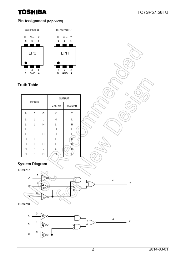
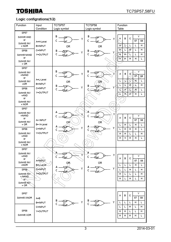
tage Single Configurable Multiple Function Gate with 3.6-V Tolerant Inputs and Outputs The TC7SP57,58 is a high performance CMOS multiple Function Gate which is guaranteed to operate from 1.2-V to 3.6-V. Designed for use in 1.5 V, 1.8 V, 2.5 V or 3.3 V systems, it achieves high speed operation while maintaining the CMOS low power dissipation. It is also designed with over voltage tolerant inputs and outputs up to 3.6 V. The output state is determined by seven patterns of 3-inputs. The user can choose the functions of XNOR(TC7SP57),XOR(TC7SP58), AND, OR, NAND,NOR, Schmitt Inverter, and Schmitt Buffer. All inputs are equippe
 TC7SP57FU Datasheet