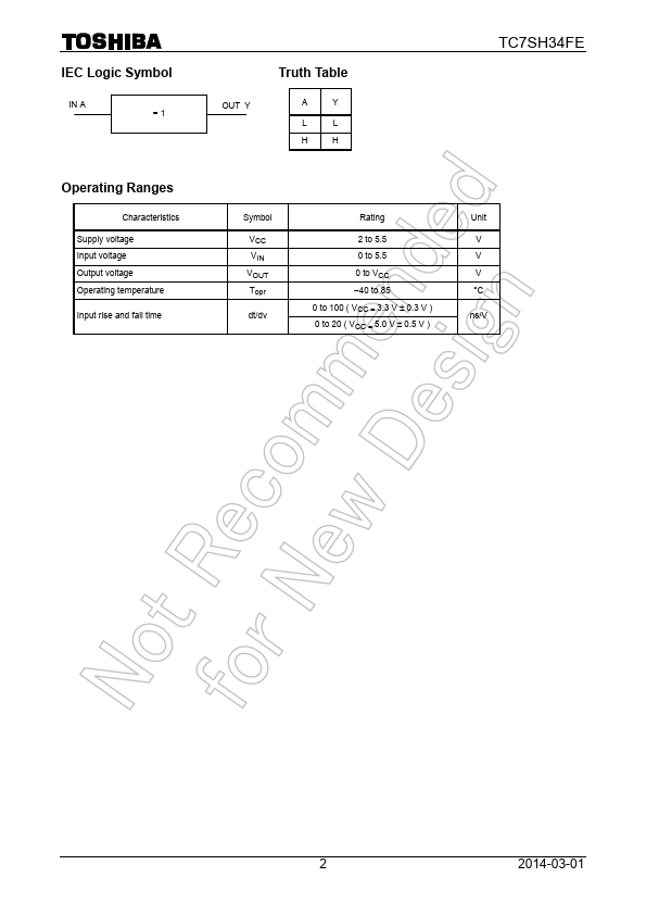
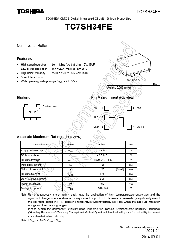
Wide operating voltage range: VCC = 2 to 5.5 V
Weight: 0.003 g (typ. )
(ESV)
Marking
HF
Product name
Pin Assignment (top view)
NC 1 IN A 2
5 VCC
GND 3
4 OUT Y
Absolute Maximum Ratings (Ta = 25°C)
Characteristics
Symbol
Rating
Unit
Supply voltage rang.
Full PDF Text Transcription for TC7SH34FE (Reference)
Note: Below is a high-fidelity text extraction (approx. 800 characters) for
TC7SH34FE. For precise diagrams, and layout, please refer to the original PDF.
TOSHIBA CMOS Digital Integrated Circuit Silicon Monolithic TC7SH34FE TC7SH34FE Non-Inverter Buffer Features • High speed operation : tpd = 3.8ns (typ.) at VCC = 5V, 15pF ...
View more extracted text
eatures • High speed operation : tpd = 3.8ns (typ.) at VCC = 5V, 15pF • Low power dissipation : ICC = 2μA (max) at Ta = 25°C • High noise immunity : VNIH = VNIL = 28% VCC (min) • 5.5-V tolerant input. • Wide operating voltage range: VCC = 2 to 5.5 V Weight: 0.003 g (typ.) (ESV) Marking HF Product name Pin Assignment (top view) NC 1 IN A 2 5 VCC GND 3 4 OUT Y Absolute Maximum Ratings (Ta = 25°C) Characteristics Symbol Rating Unit Supply voltage range DC input voltage DC output voltage Input diode current Output diode current DC output current DC VCC/ground current Power dissipation Storage temperature VCC VIN VOUT IIK IOK I
 TC7SH34FE Datasheet