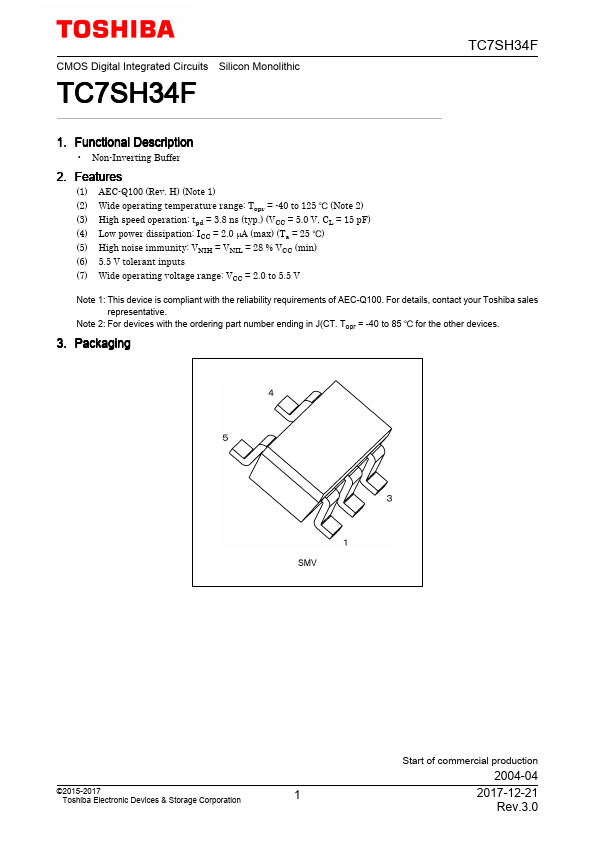
Low power dissipation ICC = 2 µA (max) at Ta = 25°C.
High noise immunity: VNIH = VNIL = 28% VCC (min).
Wide operating voltage range: VCC (opr. ) = 2~5.5 V.
5.5-V tolerant input
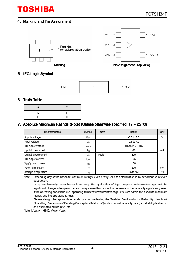
TC7SH34F TC7SH34FU
Weight SSOP5-P-0.95 : 0.016 g (typ. ) SSOP5-P-0.65A : 0.006 g (typ. )
Maximum Ratings (Ta = 25°C)
Characteristics
Supply voltage range DC input voltage DC output voltage Input diode current Output diode current.
Full PDF Text Transcription for TC7SH34F (Reference)
Note: Below is a high-fidelity text extraction (approx. 800 characters) for
TC7SH34F. For precise diagrams, and layout, please refer to the original PDF.
TC7SH34F/FU TOSHIBA CMOS Digital Integrated Circuit Silicon Monolithic TC7SH34F,TC7SH34FU NON-Inverter Features • High speed ................................. tpd = 3.8 n...
View more extracted text
er Features • High speed ................................. tpd = 3.8 ns (typ.) at VCC = 5 V • Low power dissipation .............. ICC = 2 µA (max) at Ta = 25°C • High noise immunity: VNIH = VNIL = 28% VCC (min) • Wide operating voltage range: VCC (opr.) = 2~5.5 V • 5.5-V tolerant input TC7SH34F TC7SH34FU Weight SSOP5-P-0.95 : 0.016 g (typ.) SSOP5-P-0.65A : 0.006 g (typ.) Maximum Ratings (Ta = 25°C) Characteristics Supply voltage range DC input voltage DC output voltage Input diode current Output diode current DC output current DC VCC/ground current Power dissipation Storage temperature Lead temperature (10 s) Symbol VCC V
 TC7SH34F Datasheet