The following content is an automatically extracted verbatim text
from the original manufacturer datasheet and is provided for reference purposes only.
View original datasheet text
TC74VHCT08AF/AFN/AFT/AFK
TOSHIBA CMOS Digital Integrated Circuit Silicon Monolithic
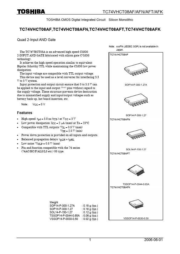
TC74VHCT08AF,TC74VHCT08AFN,TC74VHCT08AFT,TC74VHCT08AFK
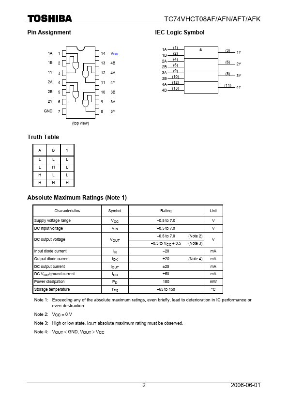
Quad 2-Input AND Gate
The TC74VHCT08A is an advanced high speed CMOS 2-INPUT AND GATE fabricated with silicon gate C2MOS technology.
It achieves the high speed operation similar to equivalent Bipolar Schottky TTL while maintaining the CMOS low power dissipation.
The input voltage are compatible with TTL output voltage. This device may be used as a level converter for interfacing 3.3 V to 5 V system. Input protection and output circuit ensure that 0 to 5.5 V can be applied to the input and output (Note) pins without regard to the supply voltage.
 TC74VHCT08AFT Datasheet