TC7SZ125AFE - CMOS Digital Integrated Circuit Silicon Monolithic
Toshiba
Key Features
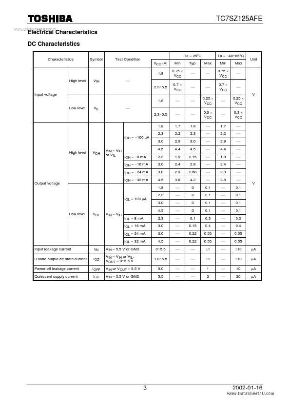
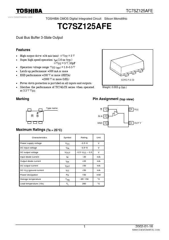
High output drive: ±24 mA (min) @VCC = 3 V Super high speed operation: tpd 2.6 ns (typ. ) @VCC = 5 V, 50pF Operation voltage range: VCC (opr) = 1.8~5.5 V Latch-up performance: ±500 mA or more ESD performance: ±200 V or more (JEITA) ±2000 V or more (MIL) Power down protection is provided on all inputs and outputs. Matches the performance of TC74LCX series when operated at 3.3 V VCC. Weight: 0.003 g (typ. )
Marking
Type name
Pin Assignment (top view)
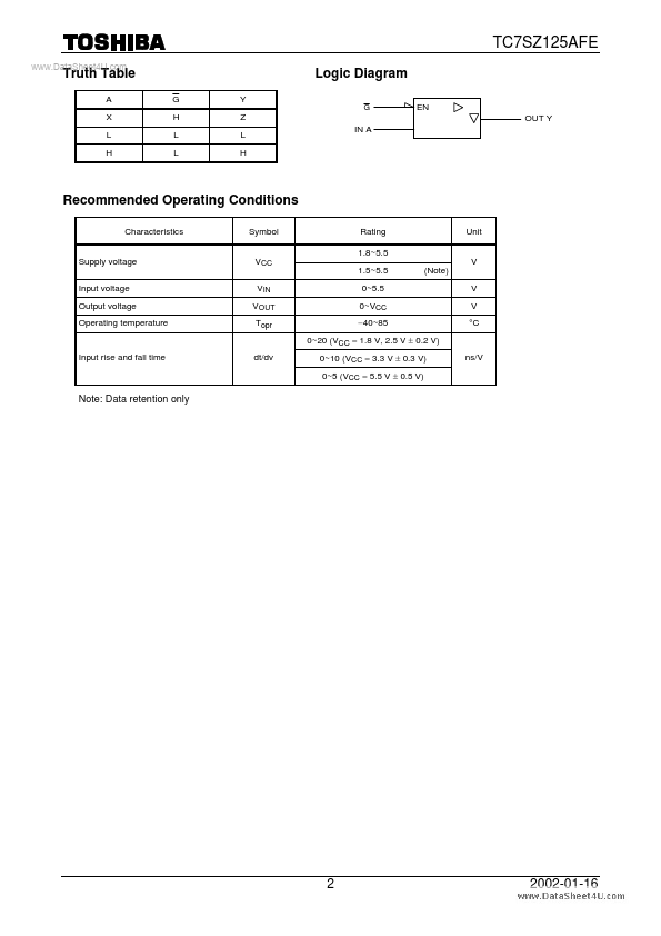
G
1.
Full PDF Text Transcription for TC7SZ125AFE (Reference)
Note: Below is a high-fidelity text extraction (approx. 800 characters) for
TC7SZ125AFE. For precise diagrams, and layout, please refer to the original PDF.
TC7SZ125AFE www.DataSheet4U.com TOSHIBA CMOS Digital Integrated Circuit Silicon Monolithic TC7SZ125AFE Dual Bus Buffer 3-State Output Features · · · · · · · High output d...
View more extracted text
FE Dual Bus Buffer 3-State Output Features · · · · · · · High output drive: ±24 mA (min) @VCC = 3 V Super high speed operation: tpd 2.6 ns (typ.) @VCC = 5 V, 50pF Operation voltage range: VCC (opr) = 1.8~5.5 V Latch-up performance: ±500 mA or more ESD performance: ±200 V or more (JEITA) ±2000 V or more (MIL) Power down protection is provided on all inputs and outputs. Matches the performance of TC74LCX series when operated at 3.3 V VCC. Weight: 0.003 g (typ.
 TC7SZ125AFE Datasheet