TC7SP3066TU - Low Voltage Dual Supply Single Bus Switch
Toshiba
Key Features
Operating voltage range: VCCA = 1.1 to 2.7 V (Control portion) VCCB = 1.65 to 3.6 V (Switch portion).
ON-resistance: RON = 8 Ω (max) (VCCB = 2.7 V) RON = 10 Ω (max) (VCCB = 2.3 V).
ESD performance: Machine model ≥ ±200 V Human body model ≥ ±2000 V.
Ultra-small package: UF6.
3.6-V tolerance function and power-down protection at the Output Enable input. Start of commercial production
2005-12
1
2014-03-01
Pin Assignment (top view)
TC7SP3066TU
VCCB.
Full PDF Text Transcription for TC7SP3066TU (Reference)
Note: Below is a high-fidelity text extraction (approx. 800 characters) for
TC7SP3066TU. For precise diagrams, and layout, please refer to the original PDF.
TC7SP3066,3067TU TOSHIBA CMOS Digital Integrated Circuit Silicon Monolithic TC7SP3066TU, TC7SP3067TU TC7SP3066TU Low Voltage Dual Supply Single Bus Switch (analog) TC7SP3...
View more extracted text
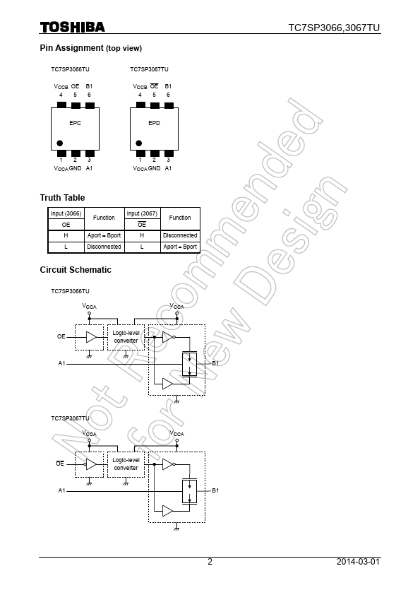
TC7SP3066TU Low Voltage Dual Supply Single Bus Switch (analog) TC7SP3067TU Low Voltage Dual Supply Single Bus Switch (analog) The TC7SP3066 and TC7SP3067 are high-speed CMOS one-bit analog bus switches with separate power supplies for control and switch portions. In the TC7SP3066, the switch is on when Output Enable (OE) is High. In the TC7SP3067, the switch is on when Output Enable ( OE ) is Low. The TC7SP3066 and TC7SP3067 support power-down protection by incorporating 3.6-V-torelant control inputs. These devices are suitable for applications where the control voltage is lower than the signal line voltage.
 TC7SP3066TU Datasheet