Datasheet Details
| Part number | TC7SP3125TU |
|---|---|
| Manufacturer | Toshiba |
| File Size | 207.18 KB |
| Description | Low Voltage/Low Power 1-Bit Dual Supply Bus Buffer |
| Datasheet |
 TC7SP3125TU Datasheet TC7SP3125TU Datasheet
|
|
|
2.
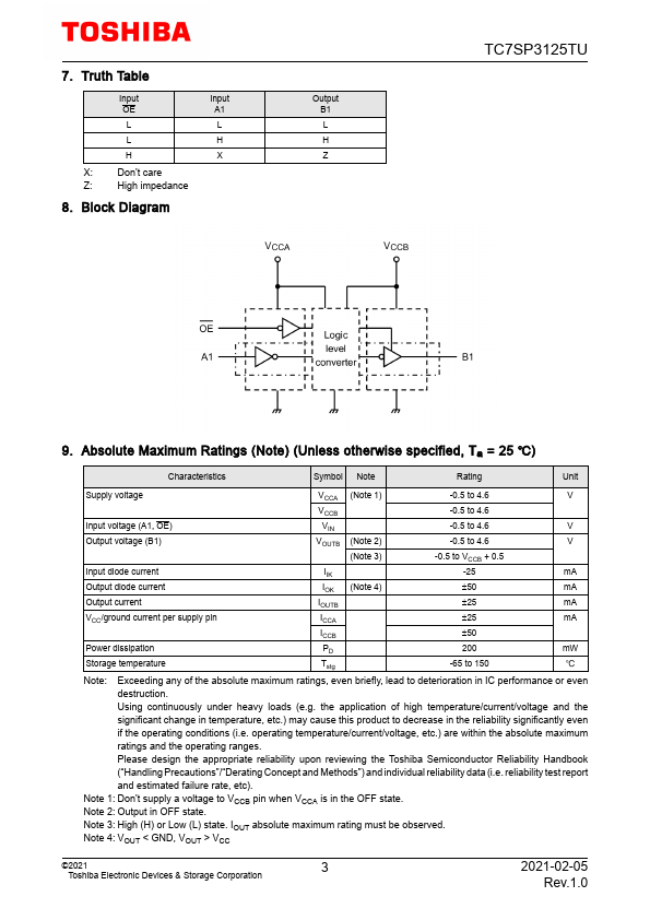
The TC7SP3125TU is an advanced high-speed CMOS 1-bit dual supply voltage interface bus buffer fabricated with silicon gate CMOS technology.
It is also designed with over voltage tolerant inputs and outputs up to 3.6 V.
| Part number | TC7SP3125TU |
|---|---|
| Manufacturer | Toshiba |
| File Size | 207.18 KB |
| Description | Low Voltage/Low Power 1-Bit Dual Supply Bus Buffer |
| Datasheet |
TC7SP3125TU Datasheet
|
|
|
|
Note: Below is a high-fidelity text extraction (approx. 800 characters) for TC7SP3125TU. For precise diagrams, and layout, please refer to the original PDF.
CMOS Digital Integrated Circuits Silicon Monolithic TC7SP3125TU TC7SP3125TU 1. Functional Description • Low-Voltage, Low-Power 1-Bit Dual-Supply Bus Buffer 2. General The...
| Brand Logo | Part Number | Description | Manufacturer |
|---|---|---|---|
| TC7SP3125CFC | 1-Bit Dual Supply Bus Buffer | Toshiba |
| Part Number | Description |
|---|---|
| TC7SP300WBG | Dual supply 2-Input NAND Gate |
| TC7SP302WBG | Dual supply 2-Input NOR Gate |
| TC7SP3066TU | Low Voltage Dual Supply Single Bus Switch |
| TC7SP3067TU | Low Voltage Dual Supply Single Bus Switch |
| TC7SP308WBG | Dual supply 2-Input AND Gate |
| TC7SP332WBG | Dual supply 2-Input OR Gate |
| TC7SP381WBG | Dual supply 2-Input Exclusive-NOR Gate |
| TC7SP386WBG | Dual supply 2-Input Exclusive-OR Gate |
| TC7SP97TU | Low Voltage Single Configurable Multiple Function Gate |
| TC7SP98TU | Low Voltage Single Configurable Multiple Function Gate |