Click to expand full text
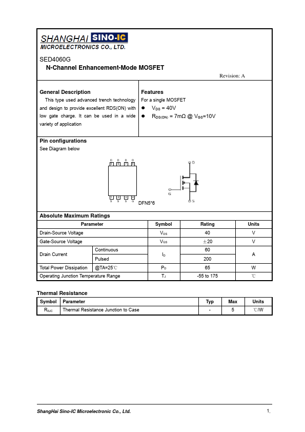
SED4060G N-Channel Enhancement-Mode MOSFET
Revision: A
General Description
This type used advanced trench technology and design to provide excellent RDS(ON) with low gate charge. It can be used in a wide variety of application
Features
For a single MOSFET
VDS = 40V RDS(ON) = 7mΩ @ VGS=10V
Pin configurations
See Diagram below
DD 56
DD 78
1 2 34
S S S G DFN5*6
Absolute Maximum Ratings
Parameter
Drain-Source Voltage
Gate-Source Voltage
Drain Current
Continuous Pulsed
Total Power Dissipation @TA=25℃
Operating Junction Temperature Range
Symbol VDS VGS
ID
PD TJ
Thermal Resistance
Symbol Parameter RθJC Thermal Resistance Junction to Case
Rating 40 ±20 60 200 65
-55 to 175
Units V V
A
W ℃
Typ Max Units - 5 ℃/W
ShangHai Sino-IC Microelectronic Co., Ltd.
1.
 SED4060G Datasheet