Click to expand full text
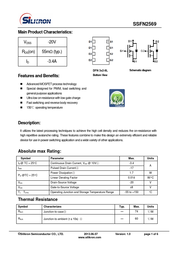
Main Product Characteristics:
VDSS RDS(on)
-20V 55mΩ (typ.)
ID -3.4A
Features and Benefits:
Advanced MOSFET process technology Special designed for PWM, load switching and
general purpose applications Ultra low on-resistance with low gate charge Fast switching and reverse body recovery 150℃ operating temperature
DFN 3x2-8L Bottom View
SSFN2569
D1 G1
G2
D2
S1 S2 Schematic diagram
Description:
It utilizes the latest processing techniques to achieve the high cell density and reduces the on-resistance with high repetitive avalanche rating. These features combine to make this design an extremely efficient and reliable device for use in power switching application and a wide variety of other applications.
 SSFN2569 Datasheet