Click to expand full text
HRLF150N10K
Jan 2016
HRLF150N10K
100V N-Channel Trench MOSFET
FEATURES
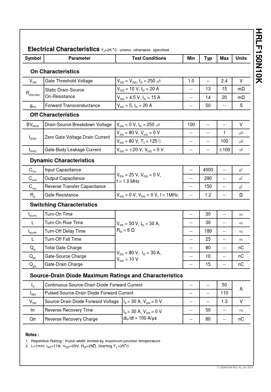
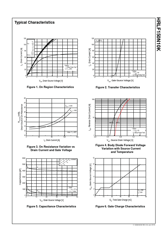
BVDSS = 100 V ID = 50 A Unrivalled Gate Charge : 80 nC (Typ.) Lower RDS(ON) : 13 Pȍ (Typ.) @VGS=10V Lower RDS(ON) : 14 Pȍ (Typ.) @VGS=4.5V 100% Avalanche Tested
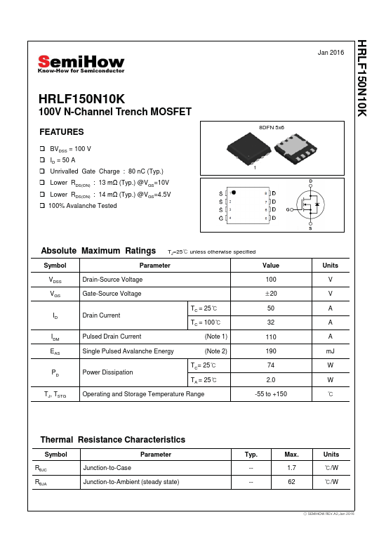
8DFN 5x6
1
Absolute Maximum Ratings TJ=25 unless otherwise specified
Symbol
Parameter
Value
VDSS VGS ID IDM EAS PD TJ, TSTG
Drain-Source Voltage
Gate-Source Voltage
Drain Current Pulsed Drain Current
TC = 25 TC = 100
(Note 1)
Single Pulsed Avalanche Energy
(Note 2)
Power Dissipation
TC= 25 TA = 25
Operating and Storage Temperature Range
100 ρ20 50 32 110 190 74 2.0 -55 to +150
Units V V A A A mJ W W
Thermal Resistance Characteristics
Symbol
Parameter
RșJC RșJA
Junction-to-Case Junction-to-Ambient (steady state)
Typ.
 HRLF150N10K Datasheet