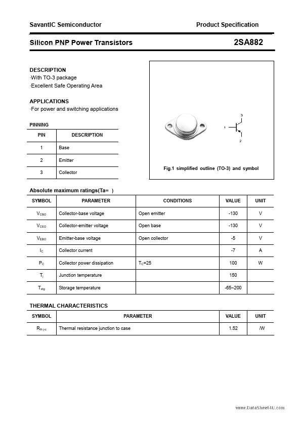
With TO-3 package
Excellent Safe Operating Area APPLICATIONS
For power and switching applications
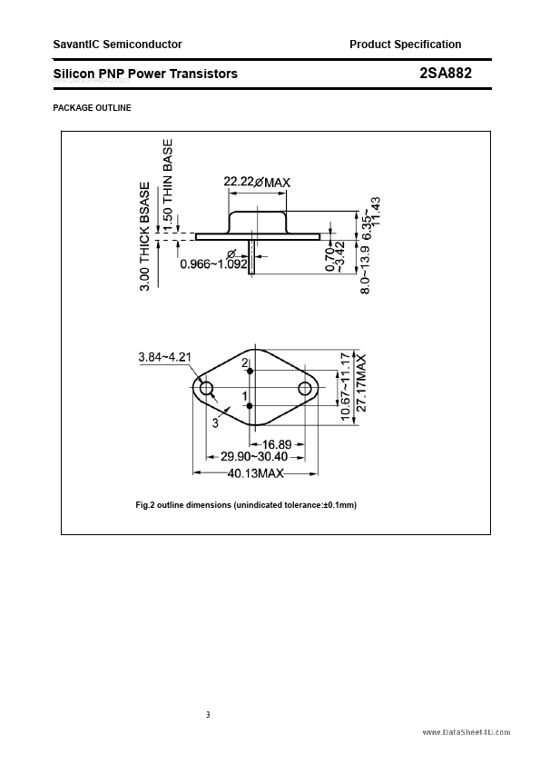
PINNING PIN 1 2 3 Base Emitter Collector Fig.1 simplified outline (TO-3) and symbol DESCRIPTION
Absolute maximum ratings(Ta= )
SYMBOL VCBO VCEO VEBO IC PC Tj Tstg PARAMETER Collector-bas
Full PDF Text Transcription for 2SA882 (Reference)
Note: Below is a high-fidelity text extraction (approx. 800 characters) for
2SA882. For precise diagrams, and layout, please refer to the original PDF.
SavantIC Semiconductor www.DataSheet4U.com Product Specification Silicon PNP Power Transistors 2SA882 DESCRIPTION ·With TO-3 package ·Excellent Safe Operating Area APPLIC...
View more extracted text
2 DESCRIPTION ·With TO-3 package ·Excellent Safe Operating Area APPLICATIONS ·For power and switching applications PINNING PIN 1 2 3 Base Emitter Collector Fig.1 simplified outline (TO-3) and symbol DESCRIPTION Absolute maximum ratings(Ta= ) SYMBOL VCBO VCEO VEBO IC PC Tj Tstg PARAMETER Collector-base voltage Collector-emitter voltage Emitter-base voltage Collector current Collector power dissipation Junction temperature Storage temperature TC=25 CONDITIONS Open emitter Open base Open collector VALUE -130 -130 -5 -7 100 150 -65~200 UNIT V V V A W THERMAL CHARACTERISTICS SYMBOL Rth j-c PARAMETER Thermal resistance junction
 2SA882 Datasheet