Datasheet Details
| Part number | K4N51163QZ |
|---|---|
| Manufacturer | Samsung Semiconductor |
| File Size | 1.37 MB |
| Description | 512Mbit gDDR2 SDRAM |
| Datasheet |
 K4N51163QZ Datasheet K4N51163QZ Datasheet
|
|
|
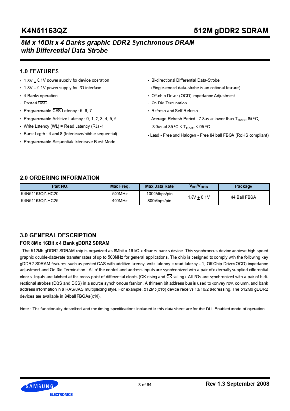
FOR 8M x 16Bit x 4 Bank gDDR2 SDRAM The 512Mb gDDR2 SDRAM chip is organized as 8Mbit x 16 I/O x 4banks banks device.
graphic double-data-rate transfer rates of up to 500MHz for general applications.
| Part number | K4N51163QZ |
|---|---|
| Manufacturer | Samsung Semiconductor |
| File Size | 1.37 MB |
| Description | 512Mbit gDDR2 SDRAM |
| Datasheet |
K4N51163QZ Datasheet
|
|
|
|
Note: Below is a high-fidelity text extraction (approx. 800 characters) for K4N51163QZ. For precise diagrams, and layout, please refer to the original PDF.
K4N51163QZ 512M gDDR2 SDRAM 512Mbit gDDR2 SDRAM 84FBGA with Halogen-Free & Lead-Free (RoHS compliant) Revision 1.3 September 2008 INFORMATION IN THIS DOCUMENT IS PROVIDED...
| Part Number | Description |
|---|---|
| K4N51163QC | 512Mbit gDDR2 SDRAM |
| K4N51163QC-ZC | 512Mbit gDDR2 SDRAM |
| K4N56163QF-GC | 256Mbit gDDR2 SDRAM |
| K4N56163QG | 256Mbit gDDR2 SDRAM |
| K4N26323AE-GC | 128Mbit GDDR2 SDRAM |