Datasheet Details
| Part number | K4J55323QF-GC16 |
|---|---|
| Manufacturer | Samsung Semiconductor |
| File Size | 1.00 MB |
| Description | 256Mbit GDDR3 SDRAM |
| Datasheet |
 K4J55323QF-GC16 Datasheet K4J55323QF-GC16 Datasheet
|
|
|
Download the K4J55323QF-GC16 datasheet PDF. This datasheet also covers the K4J variant, as both devices belong to the same 256mbit gddr3 sdram family and are provided as variant models within a single manufacturer datasheet.
The 8Mx32 GDDR3 is 268,435,456 bits of hyper synchronous data rate Dynamic RAM organized as 4 x 2,097,152 words by 32 bits, fabricated with SAMSUNG’s high performance CMOS technology.
| Part number | K4J55323QF-GC16 |
|---|---|
| Manufacturer | Samsung Semiconductor |
| File Size | 1.00 MB |
| Description | 256Mbit GDDR3 SDRAM |
| Datasheet |
K4J55323QF-GC16 Datasheet
|
|
|
|
Note: Below is a high-fidelity text extraction (approx. 800 characters) for K4J55323QF-GC16. For precise diagrams, and layout, please refer to the original PDF.
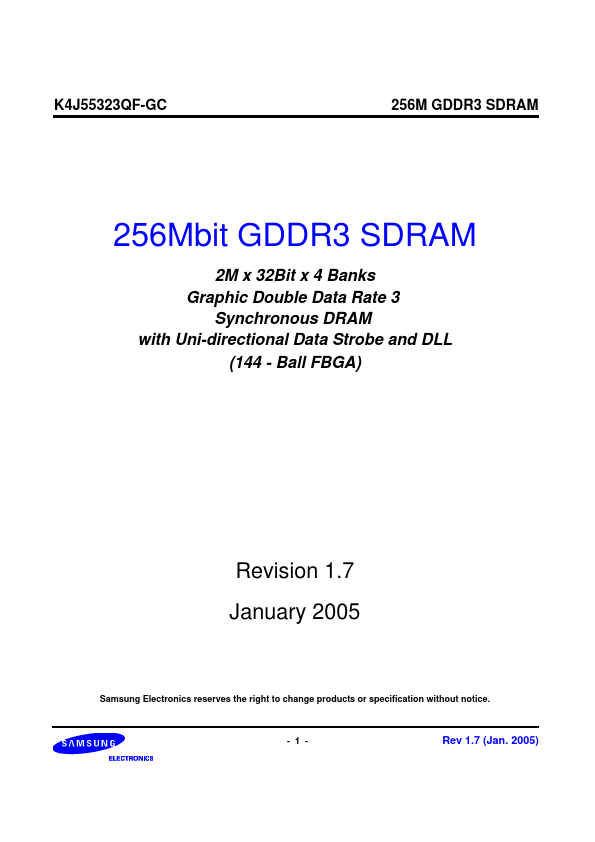
K4J55323QF-GC 256M GDDR3 SDRAM 256Mbit GDDR3 SDRAM 2M x 32Bit x 4 Banks Graphic Double Data Rate 3 Synchronous DRAM with Uni-directional Data Strobe and DLL (144 - Ball F...
| Part Number | Description |
|---|---|
| K4J55323QF-GC14 | 256Mbit GDDR3 SDRAM |
| K4J55323QF-GC15 | 256Mbit GDDR3 SDRAM |
| K4J55323QF-GC | 256Mbit GDDR3 SDRAM |
| K4J55323QF-GC20 | 256Mbit GDDR3 SDRAM |
| K4J52324QE | 512Mbit GDDR3 SDRAM |