Datasheet Details
| Part number | K9F5616Q0C |
|---|---|
| Manufacturer | Samsung Semiconductor |
| File Size | 684.12 KB |
| Description | 512Mb/256Mb 1.8V NAND Flash Errata |
| Datasheet |
 K9F5616Q0C Datasheet K9F5616Q0C Datasheet
|
|
|
Download the K9F5616Q0C datasheet PDF. This datasheet also covers the K9F variant, as both devices belong to the same 512mb/256mb 1.8v nand flash errata family and are provided as variant models within a single manufacturer datasheet.
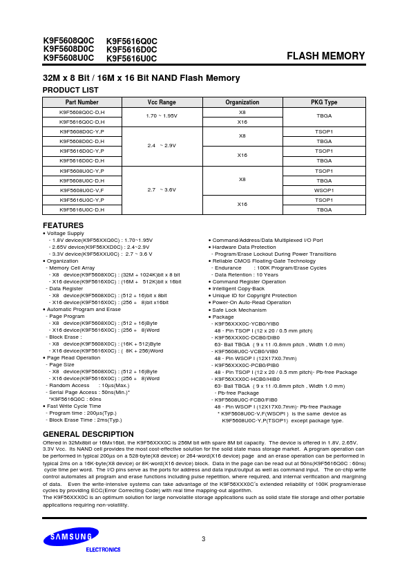
Offered in 32Mx8bit or 16Mx16bit, the K9F56XXX0C is 256M bit with spare 8M bit capacity.
The device is offered in 1.8V, 2.65V, 3.3V Vcc.
Its NAND cell provides the most cost-effective solutIon for the solid state mass storage market.
| Part number | K9F5616Q0C |
|---|---|
| Manufacturer | Samsung Semiconductor |
| File Size | 684.12 KB |
| Description | 512Mb/256Mb 1.8V NAND Flash Errata |
| Datasheet |
K9F5616Q0C Datasheet
|
|
|
|
Note: Below is a high-fidelity text extraction (approx. 800 characters) for K9F5616Q0C. For precise diagrams, and layout, please refer to the original PDF.
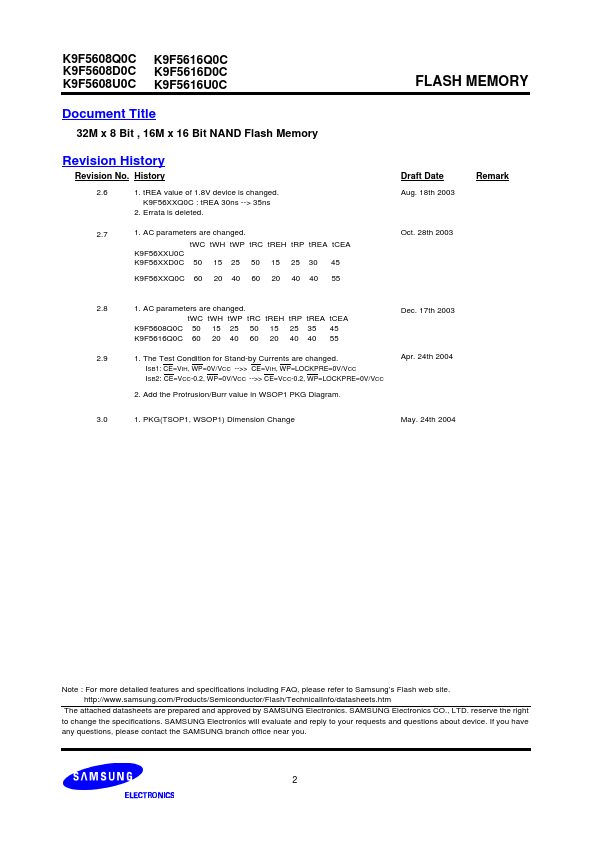
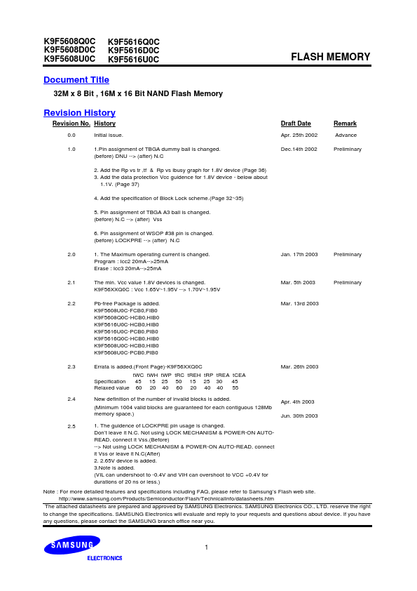
K9F5608Q0C K9F5608D0C K9F5608U0C K9F5616Q0C K9F5616D0C K9F5616U0C FLASH MEMORY Document Title 32M x 8 Bit , 16M x 16 Bit NAND Flash Memory Revision History Revision No. H...
| Brand Logo | Part Number | Description | Manufacturer |
|---|---|---|---|
| K9F5616Q0C-DCB0 | 1.8V NAND Flash Errata | Samsung | |
| K9F5616Q0C-DIB0 | 1.8V NAND Flash Errata | Samsung | |
| K9F5616Q0C-HCB0 | 1.8V NAND Flash Errata | Samsung | |
| K9F5616Q0C-HIB0 | 1.8V NAND Flash Errata | Samsung |
| Part Number | Description |
|---|---|
| K9F5616Q0B-DCB0 | 32M x 8 Bit / 16M x 16 Bit NAND Flash Memory |
| K9F5616Q0B-DIB0 | 32M x 8 Bit / 16M x 16 Bit NAND Flash Memory |
| K9F5616Q0B-HCB0 | 32M x 8 Bit / 16M x 16 Bit NAND Flash Memory |
| K9F5616Q0B-HIB0 | 32M x 8 Bit / 16M x 16 Bit NAND Flash Memory |
| K9F5616D0C | 32M x 8 Bit / 16M x 16 Bit NAND Flash Memory |
| K9F5616U0B-DCB0 | 32M x 8 Bit / 16M x 16 Bit NAND Flash Memory |
| K9F5616U0B-DIB0 | 32M x 8 Bit / 16M x 16 Bit NAND Flash Memory |
| K9F5616U0B-HCB0 | 32M x 8 Bit / 16M x 16 Bit NAND Flash Memory |
| K9F5616U0B-HIB0 | 32M x 8 Bit / 16M x 16 Bit NAND Flash Memory |
| K9F5616U0B-PCB0 | 32M x 8 Bit / 16M x 16 Bit NAND Flash Memory |