Click to expand full text
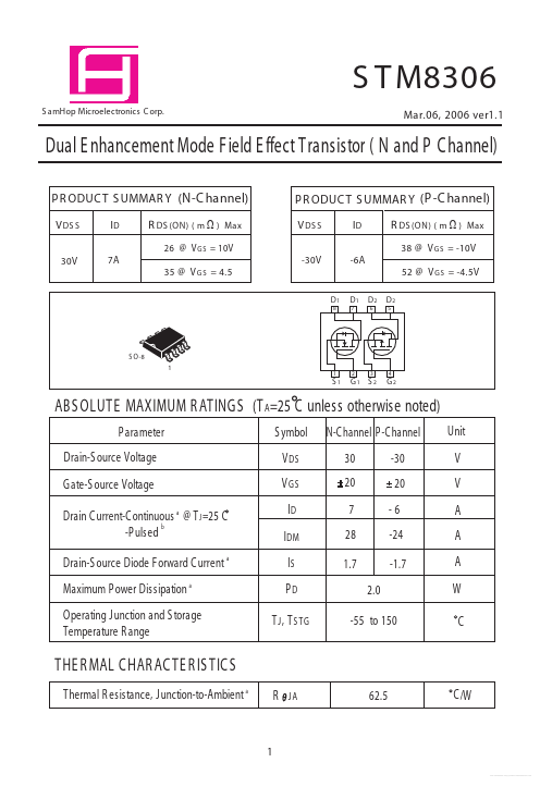
S T M8306
S amHop Microelectronics C orp.
Mar.06, 2006 ver1.1
Dual E nhancement Mode Field E ffect Transistor ( N and P Channel)
P R ODUC T S UMMAR Y (N-C hannel)
V DS S
30V
P R ODUC T S UMMAR Y (P -C hannel)
V DS S
-30V
ID
7A
R DS (ON) ( m W )
Max
ID
-6A
R DS (ON) ( m W )
Max
26 @ V G S = 10V 35 @ V G S = 4.5
D1
8
38 @ V G S = -10V 52 @ V G S = -4.5V
D1
7
D2
6
D2
5
S O-8 1
1 2 3 4
S1
G1 S 2
G2
ABS OLUTE MAXIMUM R ATINGS (T A=25 C unless otherwise noted)
P arameter Drain-S ource Voltage Gate-S ource Voltage Drain C urrent-C ontinuous a @ T J =25 C b -P ulsed Drain-S ource Diode Forward C urrent a Maximum P ower Dissipation a Operating Junction and S torage Temperature R ange S ymbol V DS V GS ID IDM IS PD T J , T S TG N-C hannel P-C hannel 30 20 7 28 1.7 2.
 STM8306 Datasheet