Datasheet Details
| Part number | TS556 |
|---|---|
| Manufacturer | STMicroelectronics |
| File Size | 339.61 KB |
| Description | Low-power dual CMOS timer |
| Datasheet |
 TS556 Datasheet TS556 Datasheet
|
|
|
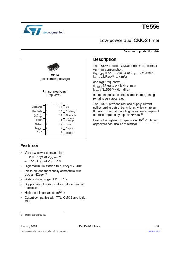
In both monostable and astable modes, timing remains very accurate.
| Part number | TS556 |
|---|---|
| Manufacturer | STMicroelectronics |
| File Size | 339.61 KB |
| Description | Low-power dual CMOS timer |
| Datasheet |
TS556 Datasheet
|
|
|
|
| Part Number | Description |
|---|---|
| TS555 | Low-power single CMOS timer |
| TS555CN | Low-power single CMOS timer |
| TS507 | High precision rail-to-rail operational amplifier |
| TS5070 | PROGRAMMABLE CODEC/FILTER COMBO 2ND GENERATION |
| TS5071 | PROGRAMMABLE CODEC/FILTER COMBO 2ND GENERATION |
| TS512 | Precision dual operational amplifiers |
| TS512A | Precision dual operational amplifiers |
| TS512B | Precision dual operational amplifiers |
| TS514 | HIGH SPEED PRECISION QUAD OPERATIONAL AMPLIFIERS |
| TS514A | HIGH SPEED PRECISION QUAD OPERATIONAL AMPLIFIERS |
The following content is an automatically extracted verbatim text from the original manufacturer datasheet and is provided for reference purposes only.