The following content is an automatically extracted verbatim text
from the original manufacturer datasheet and is provided for reference purposes only.
View original datasheet text
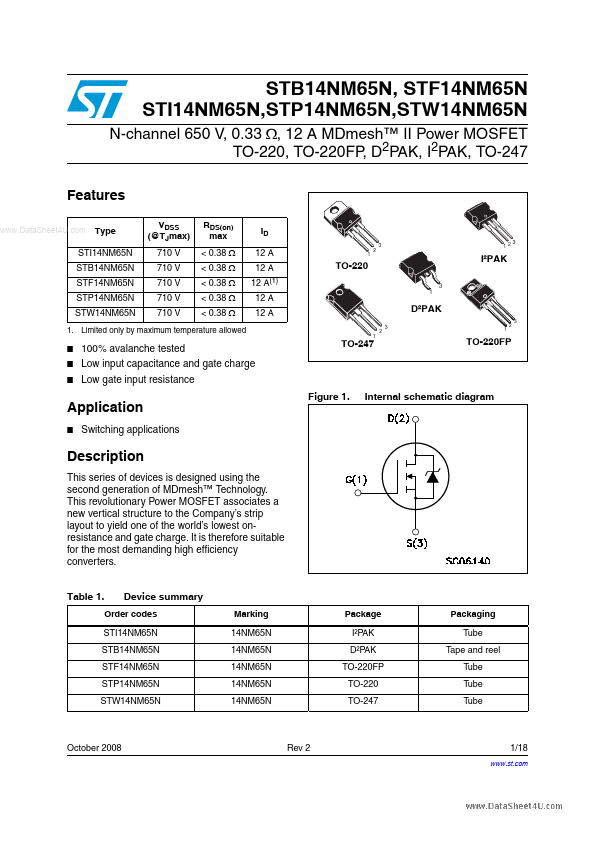
STB14NM65N, STF14NM65N STI14NM65N,STP14NM65N,STW14NM65N
N-channel 650 V, 0.33 Ω, 12 A MDmesh™ II Power MOSFET TO-220, TO-220FP, D2PAK, I2PAK, TO-247
Features
www.DataSheet4U.com
Type
VDSS (@TJmax) 710 V 710 V 710 V 710 V 710 V
RDS(on) max < 0.38 Ω < 0.38 Ω < 0.38 Ω < 0.38 Ω < 0.38 Ω
ID
3
STI14NM65N STB14NM65N STF14NM65N STP14NM65N STW14NM65N
12 A 12 A 12 A(1) 12 A 12 A
1
2
3 12
TO-220
3 1
I²PAK
D²PAK
3
1. Limited only by maximum temperature allowed ■ ■ ■
2
3
1
2
100% avalanche tested Low input capacitance and gate charge Low gate input resistance
TO-247
1
TO-220FP
Application
■
Figure 1.
Internal schematic diagram
Switching applications
Description
This series of devices is designed using the second generation of MDmesh™ Technology.
 STW14NM65N Datasheet