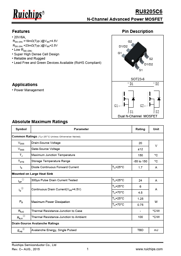
G2 D1/D2
G1
S2 D1/D2 S1
SOT23-6
D1
D2
Absolute Maximum Ratings
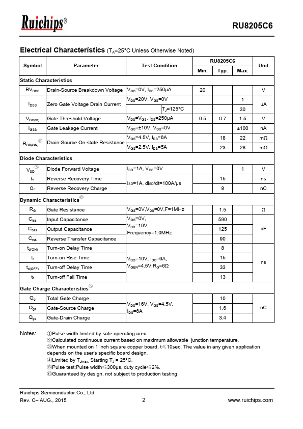
Symbol
Parameter
Common Ratings (TA=25°C Unless Otherwise Noted)
VDSS VGSS
TJ TSTG
IS
Drain-Source Voltage Gate-Source Voltage Maximum Junction Temperature Storage Temperature Range Diode Continuous Forward Current
Mounted on
The following content is an automatically extracted verbatim text
from the original manufacturer datasheet and is provided for reference purposes only.
View original datasheet text
RU8205C6
N-Channel Advanced Power MOSFET
Features
• 20V/6A, RDS (ON) =18mΩ(Typ.)@VGS=4.5V RDS (ON) =23mΩ(Typ.)@VGS=2.5V • Low RDS (ON) • Super High Dense Cell Design • Reliable and Rugged • Lead Free and Green Devices Available (RoHS Compliant)
Applications
• Power Management
Pin Description
G2 D1/D2
G1
S2 D1/D2 S1
SOT23-6
D1
D2
Absolute Maximum Ratings
Symbol
Parameter
Common Ratings (TA=25°C Unless Otherwise Noted)
VDSS VGSS
TJ TSTG
IS
Drain-Source Voltage Gate-Source Voltage Maximum Junction Temperature Storage Temperature Range Diode Continuous Forward Current
Mounted on Large Heat Sink
IDP①
300μs Pulse Drain Current Tested
ID② Continuous Drain Current(VGS=4.
 RU8205C6 Datasheet