Datasheet4U Logo Datasheet4U.com

HD74LS174P - Hex / Quadruple D-type Flip-Flops

Download the HD74LS174P datasheet PDF. This datasheet also covers the HD74LS174 variant, as both devices belong to the same hex / quadruple d-type flip-flops family and are provided as variant models within a single manufacturer datasheet.

Features

  • complementary outputs from each flip-flops. Information at the D inputs meeting the setup time requirements is transferred to the Q outputs on the positive-going edge of the clock pulse. Clock triggering occurs at a particular voltage level and is not directly related to the transition time of the positive-going pulse. When the clock input is at either the high or low level, the D input signal has no effect at the outputs. Features.
  • Ordering Information.
  • HD74LS174 Part Name.

📥 Download Datasheet

Note: The manufacturer provides a single datasheet file (HD74LS174-Renesas.pdf) that lists specifications for multiple related part numbers.

Datasheet Details

Part number HD74LS174P
Manufacturer Renesas
File Size 243.78 KB
Description Hex / Quadruple D-type Flip-Flops
Datasheet download datasheet HD74LS174P Datasheet

Full PDF Text Transcription

Click to expand full text
HD74LS174 / HD74LS175 Hex / Quadruple D-type Flip-Flops (with clear) REJ03D0451–0300 Rev.3.00 Jul.15.2005 
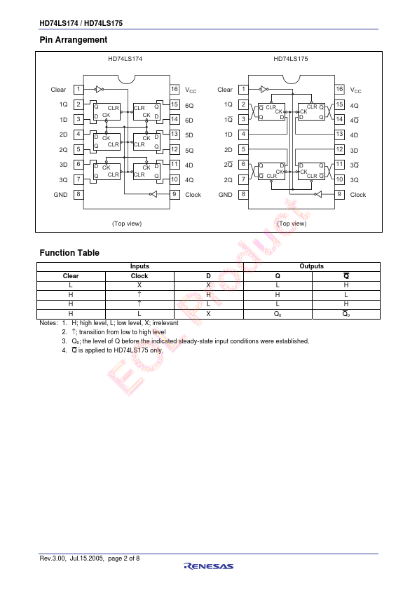
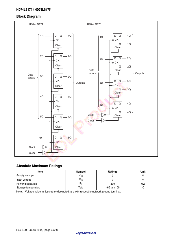
These positive-edge-triggered flip-flops utilize TTL circuitry to implement D-type flip-flop logic. All have a direct clear input, and the HD74LS175 features complementary outputs from each flip-flops. Information at the D inputs meeting the setup time requirements is transferred to the Q outputs on the positive-going edge of the clock pulse. Clock triggering occurs at a particular voltage level and is not directly related to the transition time of the positive-going pulse. When the clock input is at either the high or low level, the D input signal has no effect at the outputs.
Published: |