Datasheet4U Logo Datasheet4U.com

9QXL2001C - PCIe Clock Buffer

Description

The 9QXL2001C is an enhanced-performance 9QXL2001B with ultra-low-additive phase jitter for PCIe Gen5, Gen6 and UPI applications.

The 9QXL2001C also reduces propagation delay by approximately 50% with respect to the 9QXL2001B.

Common Clocked (CC) Independent R
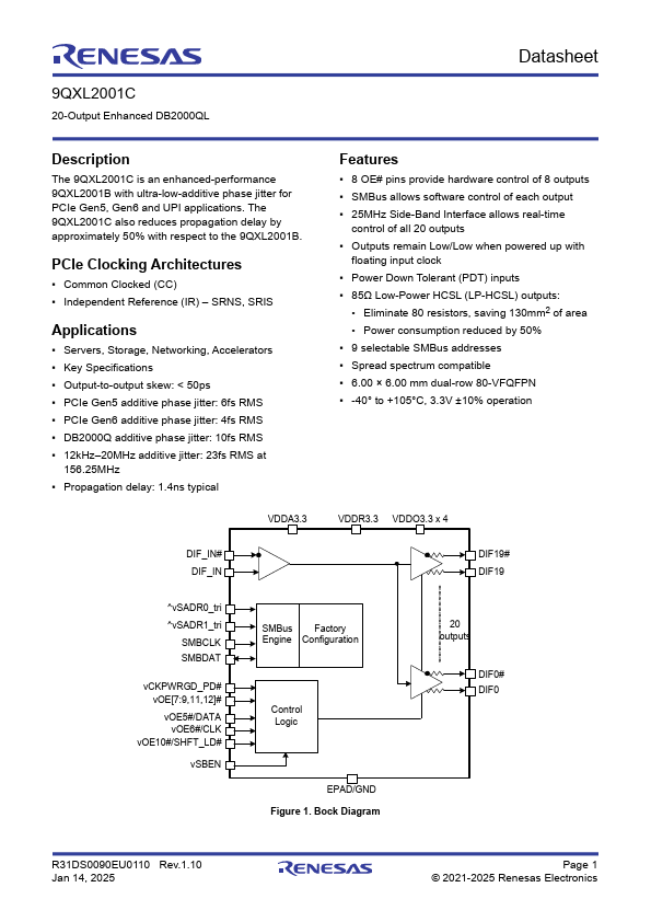
Features

  • 8 OE# pins provide hardware control of 8 outputs.
  • SMBus allows software control of each output.
  • 25MHz Side-Band Interface allows real-time control of all 20 outputs.
  • Outputs remain Low/Low when powered up with floating input clock.
  • Power Down Tolerant (PDT) inputs.
  • 85Ω Low-Power HCSL (LP-HCSL) outputs:.
  • Eliminate 80 resistors, saving 130mm2 of area.
  • Power consumption reduced by 50%.
  • 9 selectable SMBus addresses.
  • Spread spectrum compatibl.

📥 Download Datasheet

Datasheet preview – 9QXL2001C

Datasheet Details

Part number 9QXL2001C
Manufacturer Renesas
File Size 903.05 KB
Description PCIe Clock Buffer
Datasheet download datasheet 9QXL2001C Datasheet
Additional preview pages of the 9QXL2001C datasheet.
Other Datasheets by Renesas

Full PDF Text Transcription

Click to expand full text
9QXL2001C 20-Output Enhanced DB2000QL Datasheet Description The 9QXL2001C is an enhanced-performance 9QXL2001B with ultra-low-additive phase jitter for PCIe Gen5, Gen6 and UPI applications. The 9QXL2001C also reduces propagation delay by approximately 50% with respect to the 9QXL2001B. PCIe Clocking Architectures ▪ Common Clocked (CC) ▪ Independent Reference (IR) – SRNS, SRIS Applications ▪ Servers, Storage, Networking, Accelerators ▪ Key Specifications ▪ Output-to-output skew: < 50ps ▪ PCIe Gen5 additive phase jitter: 6fs RMS ▪ PCIe Gen6 additive phase jitter: 4fs RMS ▪ DB2000Q additive phase jitter: 10fs RMS ▪ 12kHz–20MHz additive jitter: 23fs RMS at 156.25MHz ▪ Propagation delay: 1.4ns typical VDDA3.
Published: |