Datasheet Details
| Part number | 9QXL2001B |
|---|---|
| Manufacturer | Renesas |
| File Size | 808.96 KB |
| Description | PCIe Clock Buffer |
| Datasheet |
 9QXL2001B Datasheet 9QXL2001B Datasheet
|
|
|
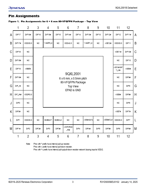
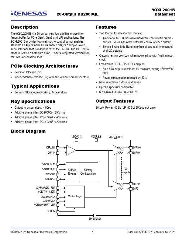
The 9QXL2001B is a 20-output very-low-additive phase jitter fanout buffer for PCIe Gen4, Gen5 and UPI applications.
The 9QXL2001B provides two methods to control output enables; standard OE# pins and SMBus enable bits, or a simple 3-wire serial interface that is independent of the SMBus.
| Part number | 9QXL2001B |
|---|---|
| Manufacturer | Renesas |
| File Size | 808.96 KB |
| Description | PCIe Clock Buffer |
| Datasheet |
9QXL2001B Datasheet
|
|
|
|