Datasheet Details
| Part number | 9DB836 |
|---|---|
| Manufacturer | Renesas |
| File Size | 613.28 KB |
| Description | 8-Output 3.3V HCSL PCIe Buffer |
| Datasheet |
 9DB836 Datasheet 9DB836 Datasheet
|
|
|
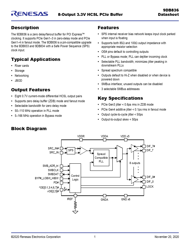
The 9DB836 is a zero delay/fanout buffer for PCI Express™ clocking.
3 in zero-delay mode and PCIe Gen14 in fanout mode.
The 9DB836 is a pin-compatible upgrade to the 9DB833 and 9DB834 with a Safe Power Sequence (SPS) clock input.
Rise| Part number | 9DB836 |
|---|---|
| Manufacturer | Renesas |
| File Size | 613.28 KB |
| Description | 8-Output 3.3V HCSL PCIe Buffer |
| Datasheet |
9DB836 Datasheet
|
|
|
|
| Part Number | Description |
|---|---|
| 9DB833 | EIGHT OUTPUT DIFFERENTIAL BUFFER |
| 9DB106 | Six Output Differential Buffer |
| 9DB1200C | Twelve Output Differential Buffer |
| 9DB1233 | 12-Output Differential Buffer |
| 9DB1904B | 19 Output Differential Buffer |
| 9DB1933 | Nineteen Output Differential Buffer |
| 9DB202 | PCI Express Jitter Attenuator |
| 9DB233 | DIFFERENTIAL BUFFER |
| 9DB306 | PCI Express Jitter Attenuator |
| 9DB401C | Four Output Differential Buffer |
The following content is an automatically extracted verbatim text from the original manufacturer datasheet and is provided for reference purposes only.