Click to expand full text
Differential-to-LVDS/0.7V Differential PCI Express™ Jitter Attenuator
8741004I
Data Sheet
General Description
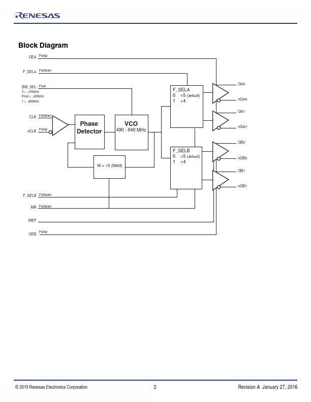
The 8741004I is a high performance Differential-to-LVDS/0.7V Differential Jitter Attenuator designed for use in PCI Express™ systems. In some PCI Express systems, such as those found in desktop PCs, the PCI Express clocks are generated from a low bandwidth, high phase noise PLL frequency synthesizer. In these systems, a jitter attenuator may be required to attenuate high frequency random and deterministic jitter components from the PLL synthesizer and from the system board. The 8741004I has 3 PLL bandwidth modes: 200kHz, 600kHz and 2MHz.
 8741004I Datasheet