Datasheet Details
| Part number | 74FCT38072S |
|---|---|
| Manufacturer | Renesas |
| File Size | 529.58 KB |
| Description | Low Skew 1 to 2 Clock Buffer |
| Datasheet |
 74FCT38072S Datasheet 74FCT38072S Datasheet
|
|
|
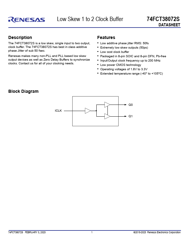
The 74FCT38072S is a low skew, single input to two output, clock buffer.
The 74FCT38072S has best in class additive phase Jitter of sub 50 fsec.
Renesas makes many non-PLL and PLL based low skew output devices as well as Zero Delay Buffers to synchronize clocks.
| Part number | 74FCT38072S |
|---|---|
| Manufacturer | Renesas |
| File Size | 529.58 KB |
| Description | Low Skew 1 to 2 Clock Buffer |
| Datasheet |
74FCT38072S Datasheet
|
|
|
|