Datasheet Details
| Part number | 6V49205B |
|---|---|
| Manufacturer | Renesas |
| File Size | 791.71 KB |
| Description | System Clock |
| Datasheet |
 6V49205B Datasheet 6V49205B Datasheet
|
|
|
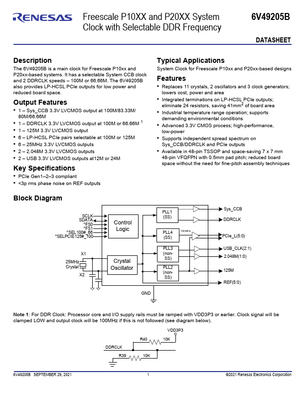
The 6V49205B is a main clock for Freescale P10xx and P20xx-based systems.
100M or 66.66M.
The 6V49205B also provides LP-HCSL PCIe outputs for low power and reduced board space.
| Part number | 6V49205B |
|---|---|
| Manufacturer | Renesas |
| File Size | 791.71 KB |
| Description | System Clock |
| Datasheet |
6V49205B Datasheet
|
|
|
|