The following content is an automatically extracted verbatim text
from the original manufacturer datasheet and is provided for reference purposes only.
View original datasheet text
Preliminary Datasheet
RJK03B9DPA
Silicon N Channel Power MOS FET Power Switching
Features
High speed switching Capable of 4.5 V gate drive Low drive current High density mounting Low on-resistance RDS(on) = 8.3 m typ. (at VGS = 10 V) Pb-free Halogen-free REJ03G1791-0320 Rev.3.20 May 12, 2010
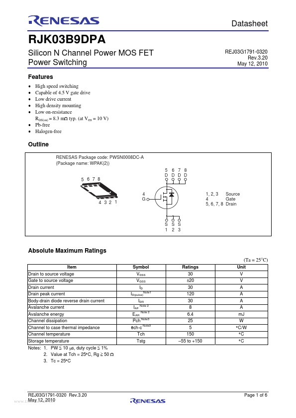
Outline
RENESAS Package code: PWSN0008DC-A (Package name: WPAK(2))
5 6 7 8 D D D D
5 6 7 8
4 G
4 3 2 1
1, 2, 3 Source 4 Gate 5, 6, 7, 8 Drain
S S S 1 2 3
Absolute Maximum Ratings
(Ta = 25°C)
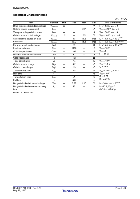
Item Drain to source voltage Gate to source voltage Drain current Drain peak current Body-drain diode reverse drain current Avalanche current Avalanche energy Channel dissipation Channel to case thermal impedance Channel temperature Storage temperature Notes: 1. PW 10 s, duty cycle 1% 2.
 RJK03B9DPA Datasheet