Datasheet Details
| Part number | RD74LVC125B |
|---|---|
| Manufacturer | Renesas Technology |
| File Size | 130.12 KB |
| Description | Quad. Bus Buffer Gates |
| Datasheet |
 RD74LVC125B Datasheet RD74LVC125B Datasheet
|
|
|
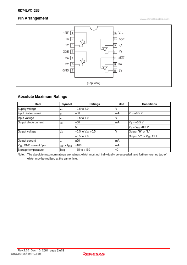
The RD74LVC125B has four bus buffer gates in a 14 pin package.
The device requires the three state control input OE to be taken high to put the output into the high impedance condition.
| Part number | RD74LVC125B |
|---|---|
| Manufacturer | Renesas Technology |
| File Size | 130.12 KB |
| Description | Quad. Bus Buffer Gates |
| Datasheet |
RD74LVC125B Datasheet
|
|
|
|