Click to expand full text
www.DataSheet4U.com
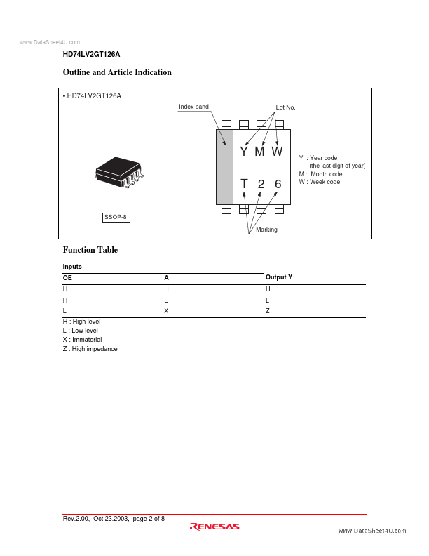
HD74LV2GT126A
Dual Bus Buffer with 3–state Output / CMOS Logic Level Shifter
REJ03D0149–0200Z (Previous ADE-205-677A (Z)) Rev.2.00 Oct.23.2003
Description
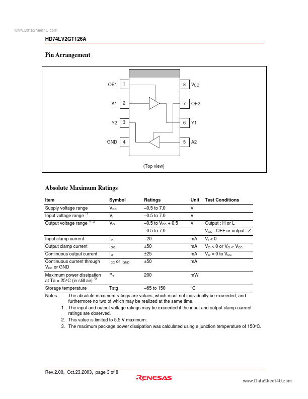
The HD74LV2GT126A has dual bus buffer with 3–state output in a 8 pin package. Output is disabled when the associated output enable (OE) input is low. To ensure the high impedance state during power up or power down, OE should be connected to GND through a pull-down resistor; the minimum value of the resistor is determined by the current souring capability of the driver. The input protection circuitry on this device allows over voltage tolerance on the input, allowing the device to be used as a logic–level translator from 3.0 V CMOS Logic to 5.0 V CMOS Logic or from 1.8 V CMOS logic to 3.
 HD74LV2GT126A Datasheet