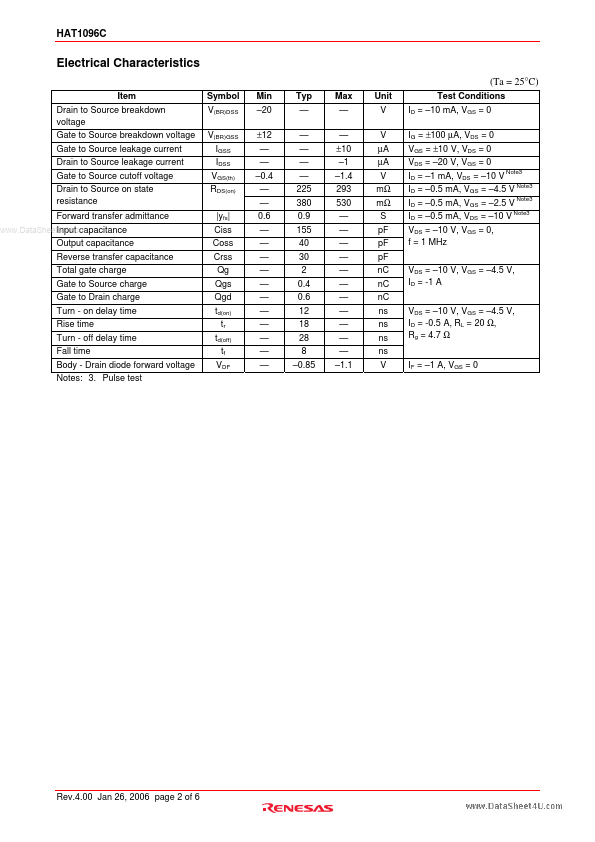
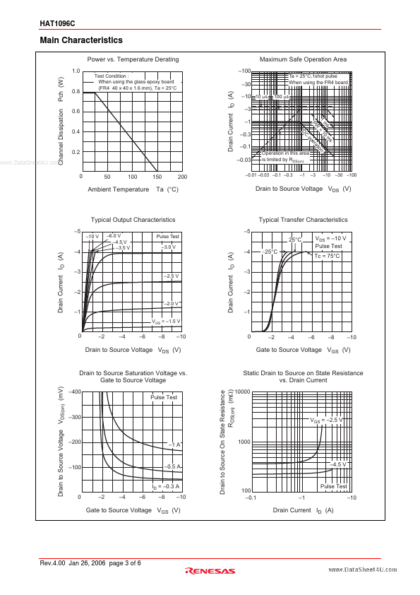
Click to expand full text
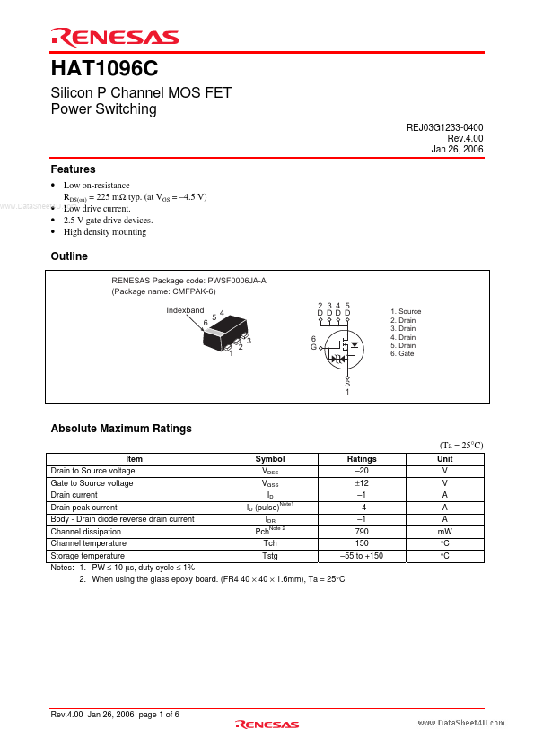
HAT1096C
Silicon P Channel MOS FET Power Switching
REJ03G1233-0400 Rev.4.00 Jan 26, 2006
Features
• Low on-resistance RDS(on) = 225 mΩ typ. (at VGS = –4.5 V) www.DataSheet4U.com • Low drive current. • 2.5 V gate drive devices. • High density mounting
Outline
RENESAS Package code: PWSF0006JA-A (Package name: CMFPAK-6) Indexband 6 5 4 6 G 2 3 4 5 D DD D
1. Source 2. Drain 3. Drain 4. Drain 5. Drain 6. Gate
1
2
3
S 1
Absolute Maximum Ratings
(Ta = 25°C)
Item Symbol Ratings Drain to Source voltage VDSS –20 Gate to Source voltage VGSS ±12 Drain current ID –1 Note1 Drain peak current ID (pulse) –4 Body - Drain diode reverse drain current IDR –1 Note 2 Channel dissipation Pch 790 Channel temperature Tch 150 Storage temperature Tstg –55 to +150 Notes: 1. PW ≤ 10 µs, duty cycle ≤ 1% 2.
 HAT1096C Datasheet