PNM6N30V12
Description
The MOSFET provide the best bination of fast switching, low on-resistance and cost-effectiveness.
VDS(V) 30
MOSFET Product Summary
RDS(on)(mΩ)
ID(A)
<15 @ VGS=10V
<20 @ VGS=4.5V
Application
- Power switching application
- Hard switched and high frequency circuits
- Uninterruptible power supply
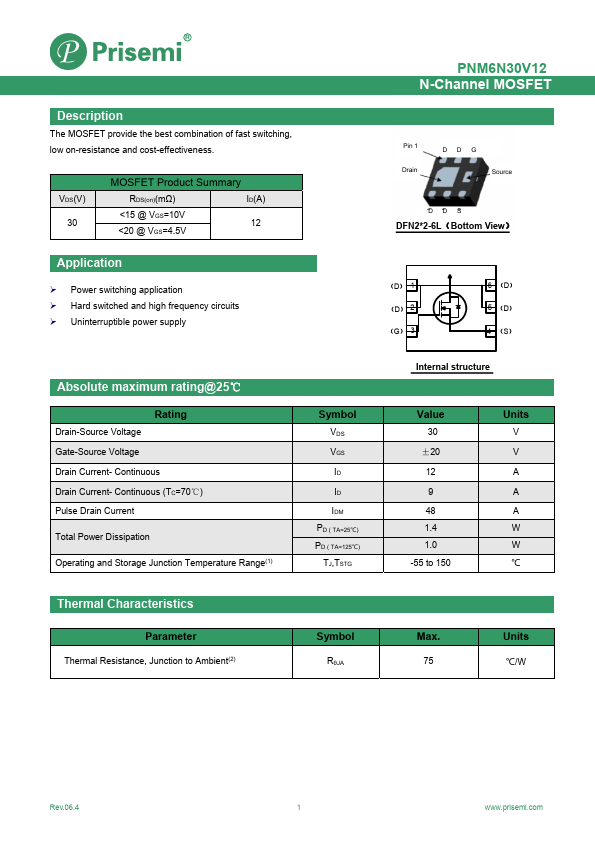
PNM6N30V12 N-Channel MOSFET
Pin 1 Drain
DDG Source
DFN2- 2-6L(Bottom View)
(D) 1 (D) 2 (G) 3
6 (D) 5 (D) 4 (S)
Absolute maximum rating@25℃
Rating
Drain-Source Voltage Gate-Source Voltage Drain Current- Continuous Drain Current- Continuous (TC=70℃) Pulse Drain Current
Total Power Dissipation
Operating and Storage Junction Temperature Range(1)
Symbol
VDS VGS ID ID IDM PD ( TA=25℃) PD ( TA=125℃) TJ,TSTG
Internal structure
Value
30 ±20
12 9 48 1.4 1.0 -55 to 150
Units
V V A A A W W ℃
Thermal Characteristics
Parameter
Thermal Resistance, Junction to Ambient(2)
Symbol
RθJA
Max....