Click to expand full text
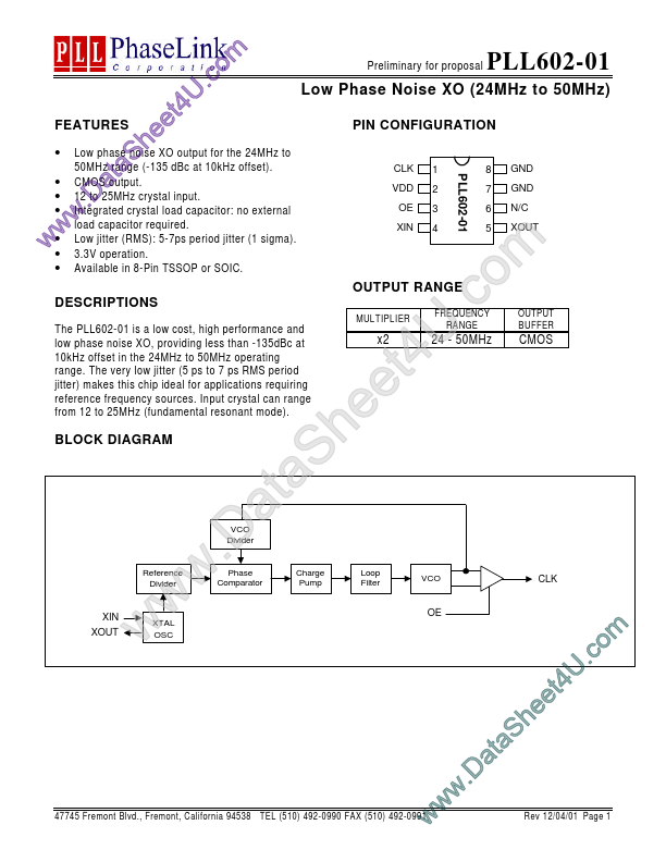
m Preliminary for proposal PLL602-01 o c . Low Phase Noise XO (24MHz to 50MHz) U t4 e FEATURES PIN CONFIGURATION e h XO output for the 24MHz to • Low phase noise S 50MHz range ta (-135 dBc at 10kHz offset). • CMOS a output. • 12 to .D25MHz crystal input. • Integrated crystal load capacitor: no external w load capacitor required. w • Low jitter (RMS): 5-7ps period jitter (1 sigma). w• 3.3V operation.
CLK 1 2 3 4 8 7 6 5 GND
PLL602-01
VDD OE
GND
N/C
•
Available in 8-Pin TSSOP or SOIC.
DESCRIPTIONS
The PLL602-01 is a low cost, high performance and low phase noise XO, providing less than -135dBc at 10kHz offset in the 24MHz to 50MHz operating range. The very low jitter (5 ps to 7 ps RMS period jitter) makes this chip ideal for applications requiring reference frequency sources.
 PLL602-01 Datasheet