Datasheet4U Logo Datasheet4U.com

PLL520-05 - (PLL520-0x) Low Phase Noise VCXO

Description

11 SEL1^ 9 8 7 6 5 GND CLKC VDD CLKT P520-0x 2 3 4 PLL520-05/-06/-07/-08/-09 www.DataSheet4U.com Low Phase Noise VCXO with multipliers (for 100-200MHz Fund Xtal) PIN DESCRIPTIONS Name XIN XOUT OE VCON GND DRIVSEL TSSOP Pin number 2 3 6 7 8,9, 10, 14 - 3x3mm QFN Pin numb

Features

  • 100MHz to 200MHz Fundamental Mode Crystal. Output range: 100.
  • 200MHz (no multiplication), 200.
  • 400MHz (2x multiplier), 400.
  • 800MHz (4x multiplier), or 800MHz.
  • 1GHz (PLL520-09 TSSOP only, 8x multiplier). High yield design supports up to 2pF stray capacitance at 200MHz. CMOS (Standard drive PLL520-07 or Selectable Drive PLL520-06), PECL (Enable low PLL520-08 or Enable high PLL520-05) or LVDS output (PLL520-09). Integrated variable capacitors.

📥 Download Datasheet

Datasheet Details

Part number PLL520-05
Manufacturer PhaseLink Corporation
File Size 275.03 KB
Description (PLL520-0x) Low Phase Noise VCXO
Datasheet download datasheet PLL520-05 Datasheet

Full PDF Text Transcription

Click to expand full text
PLL520-05/-06/-07/-08/-09 www.DataSheet4U.com 
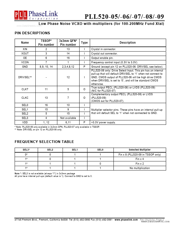
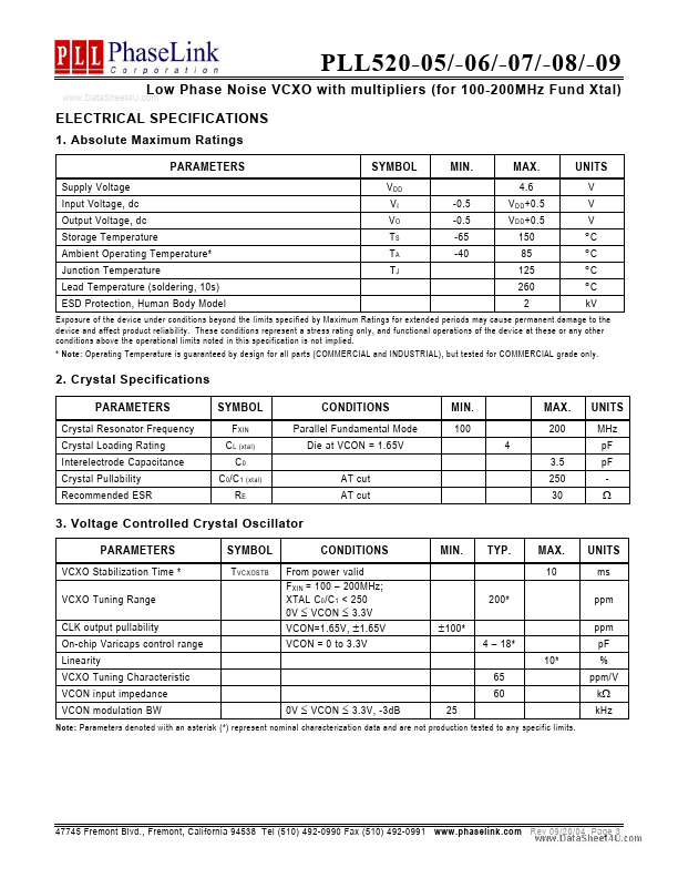
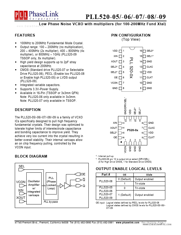
Low Phase Noise VCXO with multipliers (for 100-200MHz Fund Xtal) PIN CONFIGURATION (Top View) VDD XIN XOUT SEL3^ SEL2^ OE VCON GND 1 2 3 4 5 6 7 8 16 15 14 13 12 11 10 9 SEL0^ SEL1^ GND CLKC VDD CLKT GND GND FEATURES • • 100MHz to 200MHz Fundamental Mode Crystal. Output range: 100 – 200MHz (no multiplication), 200 – 400MHz (2x multiplier), 400 – 800MHz (4x multiplier), or 800MHz – 1GHz (PLL520-09 TSSOP only, 8x multiplier). High yield design supports up to 2pF stray capacitance at 200MHz. CMOS (Standard drive PLL520-07 or Selectable Drive PLL520-06), PECL (Enable low PLL520-08 or Enable high PLL520-05) or LVDS output (PLL520-09). Integrated variable capacitors. Supports 3.3V-Power Supply.
Published: |