Click to expand full text
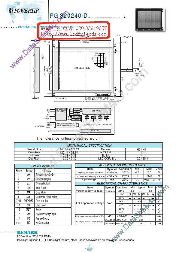
120.24 0.5 112.2 105.4 92.14(V/A) 86.37(A/A)
.c U 4 t e e h S a at .D w w w
4.44 6.63 4.02 H1 H2 9.53
7.11
PG 320240-D om
74.04 148.02 0.5 136.2 120.14(V/A) 115.17(A/A) (8.0)
OUTLINE DIMENSION & BLOCK DIAGRAM
190 10.0 CCFL
59.81
0.33 0.03 (P2.54 x 2) 5.08 Molex 50-57-9403
1
320 x 240 Dots
Vss Vdd (TEST POINT) Vee VLCD A K
Overall Size View Area Dot Size Dot Pitch
PIN ASSIGNMENT
Pin no. Symbol Vss 1 2 Vdd 3 VLCD 4 RD 5 WR Ao 6 7~14 DB0~DB7 15 CS 16 RST 17 Vee 18 FG NC 19/20
Function Power supply(GND) Power supply(+) Contrast Adjust Data Read Data Write Command / Data select Data bus line Chip select Reset Negative voltage input Frame Ground No Connection
m o .c U 4 t e e h S a t a .D w w w
20 19
0.03 0.33
1.6
HLOE4- 3.5
HOLE20- 1.0 PAD20- 1.8 139.98
(P2.54 x 9) 22.86
21.
 pg320240d Datasheet