Click to expand full text
PG 12864-O
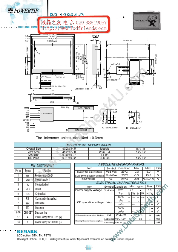
OUTLINE DIMENSION & BLOCK DIAGRAM
80.0 0.5 77.6(LCD) 73.6(V/A) 66.52(A/A) 97 0.5 6.5 5.0 77.6(PCB)
1.2 3.2 6.74 10.0MAX.
30.36 23.25
44.2
1 2- 0.6 1.0
18 27.0 100.0 3.0
9.6 8.6
18.0 8.0
A
RES CS RS WR RD D0~D7 Vdd Vo Vss A K
The tolerance unless classified
Overall Size View Area Dot Size Dot Pitch 50.2 x 34.5 45.2 x 27.0 0.28 x 0.27 0.31 x 0.32
PIN ASSIGNMENT
Pin no. Symbol Function
1 2 3 4 5 6 7 8 9~16 17 18
Power supply(GND) Power supply(+) Contrast Adjust Reset RES Chip select CS Command / data select RS Data write WR Data read RD DB0-DB7 Data bus line Power supply for LED B/L (+) A K Power supply for LED B/L ( )
Vss Vdd Vo
m o .c U 4 t e e h S a t a .D w w w
TCP IC 18 1 P1.0 x 17=17.0 19.0 72.0 Conductor side 0.3 0.5 78.0 64.0 K 78.0 B
COM 64
1.
 pg12864o Datasheet