Click to expand full text
PG 12864-A/K
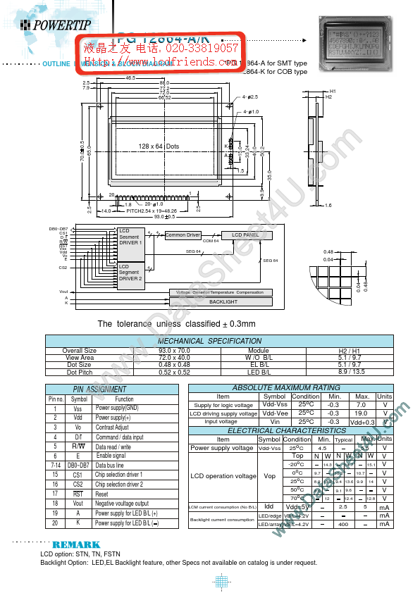
OUTLINE DIMENSION & BLOCK DIAGRAM
46.5 2.5 7.9 88.0 77.2 72.0 66.52 H1 H2
*PG 12864-A for SMT type *PG 12864-K for COB type
4- 2.5 4- 1.0
DB0~DB7 CS1 D /I R/W RST Vss Vdd Vo E CS2
Vout A K
The tolerance unless classified
Overall Size View Area Dot Size Dot Pitch 93.0 x 70.0 72.0 x 40.0 0.48 x 0.48 0.52 x 0.52
PIN ASSIGNMENT
Pin no. 1 2 3 4 5 6 7-14 15 16 17 18 19 20 Symbol Vss Vdd Vo D/I R/W E DB0~DB7 CS1 CS2 RST Vout A K
Function Power supply(GND) Power supply(+) Contrast Adjust Command / data input Data read / write Enable signal Data bus line Chip selection driver 1 Chip selection driver 2 Reset Negative voultage output
m o .c U 4 t e e h S a t a .D w w w
15.0 33.24 40.0 A 20 1 14.0 20- 1.0 1.8 PITCH2.54 x 19=48.26 93.0 0.5
4 4
70.0 0.5 65.0
9.9
35.0
1.5
50.
 pg12864ak Datasheet