Click to expand full text
PG 12864-F
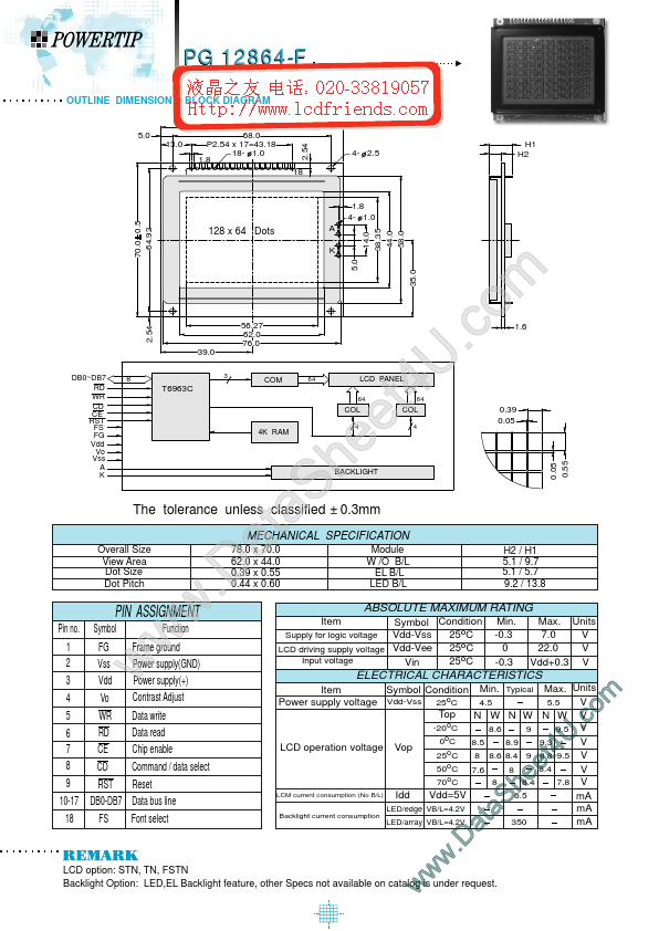
OUTLINE DIMENSION & BLOCK DIAGRAM
78.0 0.5 68.0 P2.54 x 17=43.18 18- 1.0 1.8 1
5.0 13.0
2.54
4- 2.5
H1 H2
18
70.0 0.5 64.92
1.8 4- 1.0 14.0 38.35 44.0 58.0 5.0 35.0
128 x 64 Dots
A K
DB0~DB7 RD WR CD CE RST FS FG Vdd Vo Vss A K
8
The tolerance unless classified
Overall Size View Area Dot Size Dot Pitch 78.0 x 70.0 62.0 x 44.0 0.39 x 0.55 0.44 x 0.60
PIN ASSIGNMENT
Pin no. Symbol Function
Frame ground FG 1 2 Vss Power supply(GND) 3 Power supply(+) Vdd Contrast Adjust 4 Vo 5 Data write WR Data read RD 6 Chip enable CE 7 8 Command / data select CD 9 Reset RST 10-17 DB0-DB7 Data bus line 18 Font select FS
m o .c U 4 t e e h S a t a .D w w w
39.0 56.27 62.0 76.0 2.54 1.6
3
COM
64
LCD PANEL
T6963C
64
64
COL
4
COL
4
0.39 0.05
4K RAM
BACKLIGHT
0.
 pg12864f Datasheet