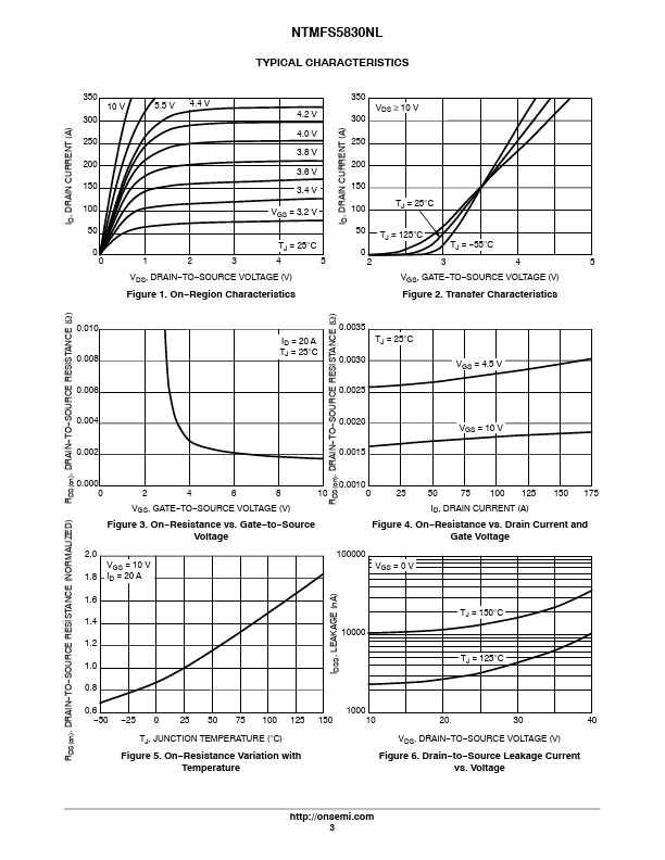
Click to expand full text
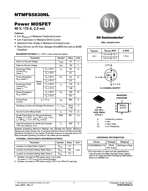
NTMFS5830NL Power MOSFET
40 V, 172 A, 2.3 mW
Features
• • • •
Low RDS(on) to Minimize Conduction Losses Low Capacitance to Minimize Driver Losses Optimized Gate Charge to Minimize Switching Losses These Devices are Pb−Free, Halogen Free/BFR Free and are RoHS Compliant
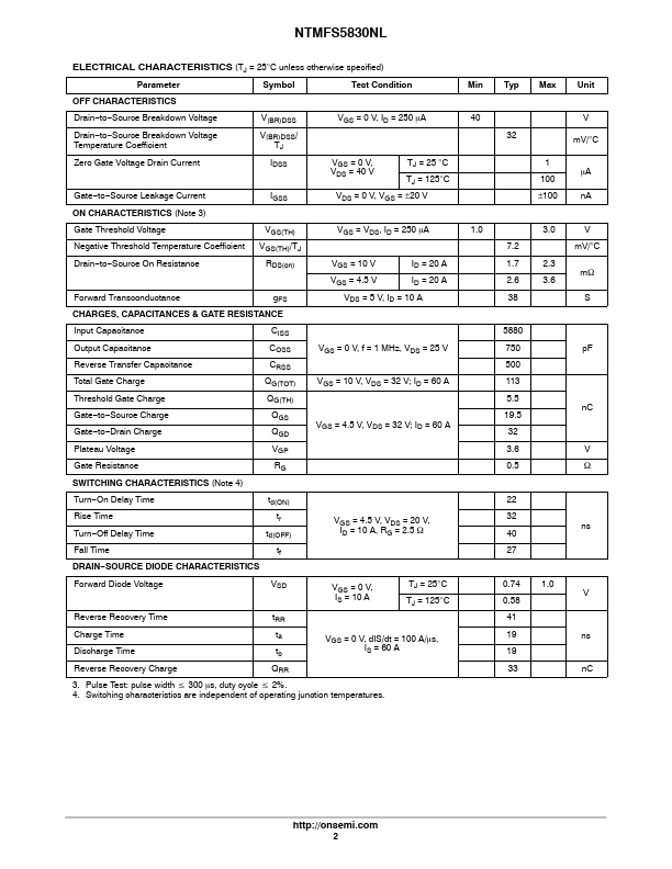
MAXIMUM RATINGS (TJ = 25°C unless otherwise stated)
Parameter Drain−to−Source Voltage Gate−to−Source Voltage Continuous Drain Current RqJA (Note 1) Power Dissipation RqJA (Note 1) Continuous Drain Current RqJC (Note 1) Power Dissipation RqJC (Note 1) Pulsed Drain Current TA = 25°C TA = 70°C TA = 25°C Steady State TA = 70°C TC = 25°C TC = 70°C TC = 25°C TC = 70°C tp = 10 ms IDM TJ, TSTG IS EAS PD ID PD Symbol VDSS VGS ID Value 40 ±20 28 22 3.2 2.
 NTMFS5830NLT1G Datasheet