Datasheet4U Logo Datasheet4U.com

NLSX5002 - Translator

Description

VCC VL GND VCC Input Voltage VL Input Voltage Ground EN Output Enable I/O VCCn I/O VLn I/O Port, Referenced to VCC I/O Port, Referenced to VL FUNCTION TABLE EN L H Operating Mode Hi Z I/O Buses Connected www.onsemi.com 3 NLSX5002 MAXIMUM RATINGS Symbol Parameter Value Conditio

Features

  • Wide VCC, VL Operating Range: 0.9 V to 4.5 V.
  • VL and VCC are independent.
  • VL may be greater than, equal to, or less than VCC.
  • High.
  • Speed with 140 Mb/s Guaranteed Date Rate for VCC, VL > 1.8 V.
  • Low Bit.
  • to.
  • Bit Skew.
  • Overvoltage Tolerant Enable and I/O Pins.
  • Non.
  • Preferential Power.
  • Up Sequencing.
  • Power.
  • Off Protection.
  • Small Packaging: UQFN8, 1.4 mm x 1.2 mm, 0.4 mm Pitch.

📥 Download Datasheet

Other Datasheets by ON Semiconductor

Full PDF Text Transcription

Click to expand full text
2-Bit 100 Mb/s Configurable Dual-Supply Level Translator NLSX5002 
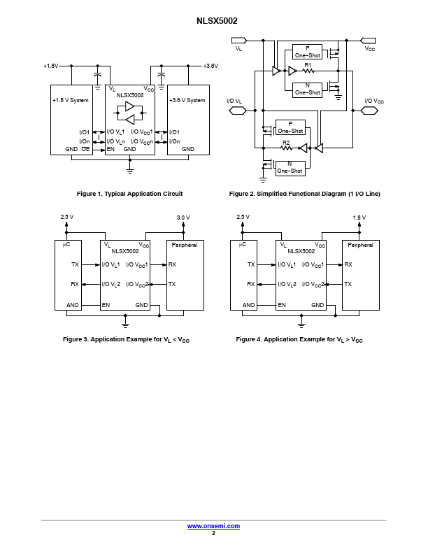
The NLSX5002 is a 2-bit configurable dual-supply autosensing bidirectional level translator that does not require a direction control pin. The I/O VCC- and I/O VL-ports are designed to track two different power supply rails, VCC and VL respectively. Both the VCC and the VL supply rails are configurable from 0.9 V to 4.5 V. This allows a logic signal on the VL side to be translated to either a higher or a lower logic signal voltage on the VCC side, and vice-versa. The NLSX5002 offers the feature that the values of the VCC and VL supplies are independent. Design flexibility is maximized because VL can be set to a value either greater than or less than the VCC supply.
Published: |